- On September 24, 2025
- In blog
PCB Solder Masks Guideline: Types, Paste Mask Differences, and DFM Insights
In PCB manufacturing, the primary role of the solder mask is to prevent solder bridges, protect copper traces, and enhance the assembly yield. However, not all solder masks are the same.
Selecting the right solder mask is important for different applications, as it directly affects the product’s durability and ease of manufacturing. How should you choose the appropriate solder mask? What design considerations should you keep in mind? These elements can influence the final outcome.
In this guide, we will provide an overview of common types of solder masks, explain the differences between PCB solder masks and paste masks, highlight key design factors, and help you make the best choice effortlessly.
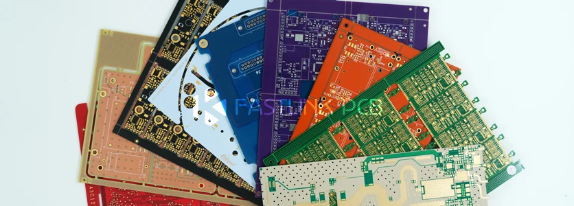
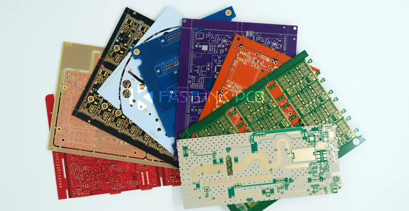
Types of PCB Solder Masks
The four solder mask types listed below are the most commonly used. By comparing their pros and cons, you can better understand their unique features.
1.Liquid Photoimageable (LPI) Solder Mask
The LPI solder mask is the most widely used type today. It is applied as a liquid to the PCB and then imaged using ultraviolet (UV) light. This method is ideal for most rigid PCBs, HDI PCBs, and designs that require high precision. The LPI solder mask offers a smooth and consistent surface, making it perfect for fine-pitch components. It boasts high resolution and is suitable for large-scale production. However, it demands precise control over the UV imaging process and is not suitable for PCBs with heavy copper or highly uneven surfaces.
2.Epoxy Screen-Printed Solder Mask
The epoxy screen-printed solder mask is a more traditional and cost-effective technique. It applies thermoset epoxy resin ink to the PCB using a stencil, making it suitable for simple, low-density designs or non-critical consumer applications. While the process is straightforward and budget-friendly, it offers lower resolution and is not ideal for fine-pitch components. For large-scale production, it also tends to be slower, which may reduce overall efficiency.
3.Dry Film Solder Mask
The dry film solder mask is typically used in applications where thickness consistency is critical. The process involves laminating a dry film onto the PCB, which is then exposed to ultraviolet (UV) light. This type of solder mask offers uniform thickness and exceptional clarity, making it ideal for high-reliability applications and designs that require precise spacing, such as fine-pitch components. While it delivers outstanding clarity, it comes with a higher material cost and is less flexible than LPI and epoxy resin masks.
4.Flexible Solder Mask
The flexible solder mask is specially designed for flexible PCBs and dynamic applications. It is often an LPI variant applied to polyimide or PET substrates, capable of withstanding repeated bending without cracking. This makes it perfect for flexible circuits, wearable tech, or any designs that need to bend during use. Although it provides excellent flexibility and is compatible with SMT processes, its application and curing require high precision, and the material cost is relatively high.
| Solder Mask Type | Advantages | Disadvantages |
| LPI Solder Mask | High resolution Suitable for mass production | Requires UV imaging and cleanroom conditions Not suitable for very thick copper Not suitable for PCBs with uneven surfaces |
| Epoxy Screen-Printed Solder Mask | Low cost Simple process, no photolithography required | Poor precision Relatively slow speed |
| Dry Film Solder Mask | Excellent clarity Excellent dielectric strength | Higher cost Poor flexibility |
| Flexible solder mask | Excellent flexibility | Higher cost |
Difference Between PCB Solder Mask and Paste Mask
When discussing PCB solder mask, one may also mention paste mask. While it’s widely understood that these represent two entirely distinct layers, what exactly are the differences between them?
Solder Mask Layer
The PCB solder mask, often referred to as the green layer, covers the PCB pads (including surface-mount pads, through-hole pads, and vias). Its primary function is to prevent solder from flowing to areas where it shouldn’t, especially during wave soldering or reflow soldering. Essentially, the areas covered in green are the solder mask. Typically, the solder mask is applied in two layers: the Top Layer and the Bottom Layer.
The solder mask leaves the pads that need to be soldered exposed, but these openings are usually slightly larger than the actual pads, creating the small circles or squares that are commonly seen. When generating gerber files, you can see the actual layout of the solder layer.
Paste Mask Layer
Also known as the solder paste or stencil layer, the paste mask is mainly used for soldering surface-mount (SMD) components. It ensures the correct amount of solder paste is applied by creating a stencil. During soldering, the stencil is placed over the PCB, aligned with the pads, and solder paste is applied. Any excess solder paste is scraped off, the stencil is removed, and then the SMD components are placed onto the solder paste and soldered in a reflow oven. The holes in the stencil are usually smaller than the pads, and the size of the paste mask holes can be adjusted to increase or decrease the paste coverage.
Key Differences Between the Two
1.The solder mask defines where the green coating is not applied and is not related to whether solder is used. The paste mask defines where solder paste should be applied, regardless of whether there is green solder mask.
2.The solder mask is a negative layer, showing where the green mask is absent; while the paste mask is a positive layer, showing where solder paste should be applied. Essentially, they are opposites.
Design Considerations
1.If pads, marker points, test points, etc., need to have solder applied, both the solder mask and paste mask should be used together.
2.If only copper needs to be exposed without solder, such as for mechanical mounting holes, only the solder mask is necessary.
3.For areas that don’t require copper exposure, like signal traces, ground planes, or vias that are covered by solder mask, when using design software, it’s unnecessary to define both the solder mask and paste mask.
DFM Insights for PCB Solder Mask
1.Tent Via Design
Objective: To minimize the exposed annular area on the PCB surface.
Method: By applying a solder mask over the via, the surrounding annular area is covered, preventing the via from being exposed.
Advantages: This helps reduce solder bridges and paste migration, particularly at pad edges or BGA patterns, and protects the PCB surface from potential damage.
2.Choosing Solder Mask Mesh Width
Objective: To ensure sufficient solder mask coverage and prevent short circuits or electrical issues.
Method: For green solder masks, set the mesh width to 4 mils, and for other colors, use 5 mils. Make sure there is at least 1 mil of solder mask coverage between the mask and the traces.
3.Solder Mask Opening to Pad Size Ratio
Objective: To ensure pads are properly protected while avoiding unnecessary copper exposure.
Method: The solder mask opening should have a 1:1 ratio with the pad size.
Note: Manufacturers may adjust the ratio based on their specific processes, and the opening can be customized according to your needs. Be especially cautious when dealing with complex geometries (e.g., sharp corners), as some solder mask coverage may be missing in these areas.
Unsure How to Begin Your PCB Manufacturing Project?
Whether it’s designing the PCB solder mask, selecting the right solder mask process, or manufacturing the PCB, FastlinkPCB provides comprehensive expert support. Since 2009, we’ve been delivering high-quality PCB solutions to businesses of all sizes. With extensive experience and advanced technology, FastlinkPCB is here to ensure your project’s success. Reach out to us today to learn more about our services and let us offer the ideal PCB solution for your electronic project!