- [email protected] Mon-Sun 0. 00-23. 59
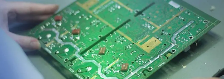
Before manufacturing a batch of fully functional PCBs, prototype PCBs are created. This crucial step in the product development cycle allows OEMs to thoroughly evaluate the electrical connections, component placement, and overall functionality of the PCB design. By testing a prototype PCB, potential issues can be identified and rectified before mass production, preventing costly errors and ensuring the success of the final PCB batch. A prototype PCB serves as a replica of the actual PCBs, either in a non-functional or fully functional form. At Fastlink, we regard the prototype PCB assembly process as a critical step in the product development cycle.
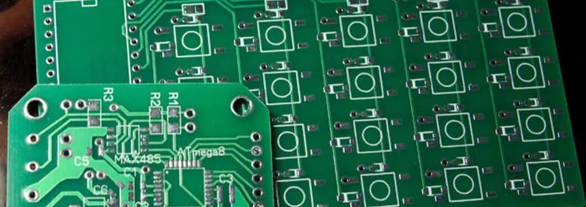
A prototype board, often referred to as a breadboard, serves as a foundational tool for assembling and testing electronic circuits. It is composed of a grid of holes or sockets designed to hold electronic components and wires, facilitating the creation of temporary circuit connections without the need for soldering. These boards are available in various types, including solderless breadboards, perfboards, and stripboards, each offering distinct benefits and suited for specific applications.
The primary function of prototype boards is to enable the assembly of electronic components and wires, forming a complete circuit. Connections are typically established using jumper wires, which are convenient for insertion and removal, minimizing the risk of damaging the components. This adaptable setup allows for experimentation with various circuit layouts, troubleshooting, and modifications, all without the permanence of a soldered connection.
Prototype PCB assembly plays a vital role after the PCB design stage, serving to validate the design’s practicality and uncover any potential problems. In this stage, manufacturers conduct a thorough evaluation of the board’s strengths and weaknesses, providing valuable insights for future iterations. This step is essential in the PCB manufacturing process, allowing for a detailed understanding of the entire procedure and the opportunity to rectify any mistakes before entering large-scale production. Through meticulous testing in the prototype phase, manufacturers aim to ensure that the final product performs reliably in mass production.
Typically, a prototype PCB is a basic version of the eventual production board, often missing complex features and design enhancements. Nevertheless, it is imperative that it be an accurate, high-quality, and fully functional test model of the final PCB. The prototype assembly process must closely mirror the essential design, functionality, and component arrangement of the final production to minimize differences.
Overlooking errors or omissions at this stage can lead to substantial costs if not addressed before moving to full-scale PCB manufacturing. Therefore, the precision and accuracy in executing a PCB prototype are crucial.
Prototype assembly allows for the practical testing of the PCB design. It helps in verifying that the board functions as intended and adheres to the required specifications. This step is crucial in validating the design before proceeding to mass production.
Prototyping helps in identifying design errors or flaws at an early stage. This early detection saves time and resources, as making corrections in a prototype is far more cost-effective than making changes during or after mass production.
Investing in prototype assembly can be a cost-saving measure in the long run. It minimizes the risk of costly errors and extensive rework that can arise from directly jumping into full-scale production without a test run.
Prototypes allow for comprehensive functionality tests, including stress testing under different conditions. This ensures that the final product will perform reliably under various real-world scenarios.
Through iterative prototype testing, designers can refine and optimize the PCB for better performance. This process can lead to enhancements in efficiency, speed, power consumption, and overall effectiveness of the PCB.
Prototype assembly provides an opportunity to assess the suitability of materials and components. It’s a practical approach to test various components to see which ones perform best, leading to better material choices in the final product.
Prototyping allows for the integration of feedback from engineers, stakeholders, and end-users. This collaborative approach can lead to design improvements and ensure that the final product meets user expectations.
By identifying and fixing issues early in the development process, prototype assembly can accelerate the product development cycle, reducing the overall time-to-market.
Prototypes can be used to check compliance with industry standards and certifications before mass production. This is crucial in industries where compliance with specific standards is mandatory.
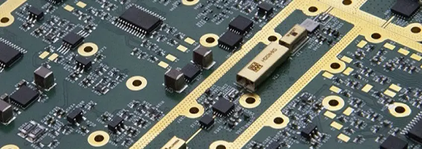
The PCB prototyping phase involves creating a physical representation of the PCB design to test its electrical connections, component placement, and overall functionality. This iterative process allows for identifying and rectifying any design flaws before committing to mass production.
The PCB prototyping process begins with converting the schematic diagram, which represents the electrical connections between components, into a PCB layout using specialized software. This layout defines the physical arrangement of components on the PCB board.
The PCB layout is then translated into Gerber files, a set of industry-standard files that contain all the necessary information for PCB fabrication. These files specify the copper traces, component placement, and drill holes on the PCB board.
The Gerber files are sent to a PCB fabrication house, where the PCB board is physically manufactured using a multi-step process. This process typically involves:
● Panel Preparation: The PCB design is transferred onto a copper sheet using photoresist, a light-sensitive material.
● Etching: The copper sheet is immersed in a chemical solution that removes the copper where the photoresist is absent, leaving behind the desired copper traces.
● Drilling: Holes for component placement and mounting are drilled into the PCB board.
● Solder Mask Application: A solder mask, a protective layer that prevents solder from adhering to unwanted areas, is applied to the PCB board.
● Silkscreen Printing: Component identifiers and other markings are printed onto the PCB board.
While the PCB board is being fabricated, the electronic components required for the PCB assembly are procured. This involves sourcing the correct components from suppliers and ensuring they meet the design specifications.
Once the PCB board and components are ready, the PCB assembly phase commences. This process involves physically placing the components onto the PCB board and soldering them into place to create the functional electronic circuit.
A stencil is used to apply solder paste, a sticky flux-filled solder, to the PCB board at the locations where the components will be placed.
The electronic components are carefully placed onto the PCB board, ensuring they are aligned correctly with the solder paste dots.
For automated assembly, a pick-and-place machine precisely positions the components onto the PCB board.
Looking for the top quality replica watches? Look no further than https://aaawatchreplica.com/. Our store offers AAA replica watches that are indistinguishable from the real thing, at a fraction of the cost. With a wide selection of luxury brands to choose from, you can find the perfect watch to fit your style and budget. Shop now and experience the ultimate in replica watch quality!
The PCB board with components is passed through a reflow oven, where the solder paste melts and forms strong bonds between the components and the PCB board.
The PCB board is cleaned to remove any residual flux or solder paste.
The assembled PCB board undergoes a thorough visual inspection to ensure proper component placement and soldering quality. Electrical testing is also performed to verify the functionality of the circuit.
For applications requiring protection from harsh environments, a conformal coating, a protective layer that insulates the PCB board from moisture, dust, and other contaminants, can be applied.
The assembled, inspected, and tested PCB boards are packaged and shipped to the customer or manufacturer for integration into the final product.
Our Prototype PCB Assembly service streamlines the process of turning intricate circuit designs into functional prototypes, eliminating the need for you to manage PCB assembly intricacies. Our manufacturing facility’s unique layout seamlessly integrates both automated and manual parts-loading stations, ensuring efficient and adaptable assembly. Our skilled personnel are adept at handling fine-pitch components and BGAs for high-density FR-4 PCBs, capable of producing prototype PCB assemblies in volumes ranging from 1 to 25 units.
At the prototype stage, our primary focus is Turn-Key circuit board assembly. Our team of expert engineers has established comprehensive guidelines for each phase of the PCB manufacturing process, enabling our clients to reap the benefits of our PCB prototyping, parts sourcing, and PCB assembly services. Additionally, we offer a partial turnkey option, where we assemble component kits according to your specifications.
Our PCB Assembly service encompasses parts procurement, allowing you to focus on your core expertise – layout design. Our dedicated sourcing team collaborates with multiple suppliers and distributors to secure components as per your requirements, ensuring efficient and cost-effective procurement. We employ advanced processes to optimize packaging selection (cut tape, tube, bulk, etc.), minimizing overall costs. Furthermore, our cross-referencing capabilities enable us to locate hard-to-find and obsolete components. Rest assured, Fastlink only substitutes components with high-quality alternatives specified in the BOM, maintaining the integrity of your original layout design. Part substitutions are strictly subject to your approval.
At Fastlink, we understand the critical role PCB assemblies play in your product development cycle. Our Prototype PCB Assembly service provides the expertise and resources you need to transform your design concepts into tangible prototypes, paving the way for successful product realization.
At Fastlink, we recognize the importance of rapid prototype PCB assembly and timely delivery for our customers. Consequently, we have optimized our turnkey assembly service for maximum efficiency. Following DFM verification, PCB manufacturing commences as soon as component sourcing is finalized. During this phase, we proactively address any PCB engineering questions (EQ) or component-related concerns before the assembly process begins. To ensure quality, open and consistent communication throughout your electronic assembly project is essential. This period also provides an opportunity to gain a deeper understanding of Fastlink’s capabilities.
Once all preparations, including bare PCBs, IPQC-approved components, stencil fabrication, and SMT machine setup are complete, the prototype PCB assembly commences. The turnkey assembly process typically takes 10-14 days; less if there are no hard-to-find components or documentation errors.
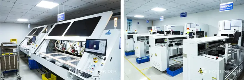
Fastlink operates two primary PCB assembly factories, encompassing a total area of 20,000 square meters. These facilities are dedicated to both prototyping and mass production of PCB assemblies. Equipped with 32 cutting-edge fully automated assembly lines, Fastlink delivers a daily production capacity exceeding 90 million parts, catering to small, medium, and large volumes. The factories are also equipped with in-house Automated Optical Inspection (AOI), X-ray inspection, and testing capabilities, ensuring a high standard of quality control.
There are more pictures of our factory’s equipment display in our company profile, please click here.