- [email protected] Mon-Sun 0. 00-23. 59
Successful PCB assembly requires more than just knowing components and assembly techniques. It demands expertise in printed circuit board design, layout, fabrication, and understanding the final product’s applications. High-quality PCB assembly services are crucial for delivering a perfect product on the first try, eliminating rework and errors.
Fastlink offers a comprehensive solution for all your circuit board production needs, encompassing fabrication, testing/inspections, and assembly. For a complete turn-key experience, we handle everything from manufacturing the PCBs and procuring components to order tracking, continuous quality monitoring, and final assembly. Alternatively, for partial turn-key projects, you can provide the PCBs and some components, and we’ll handle the rest.
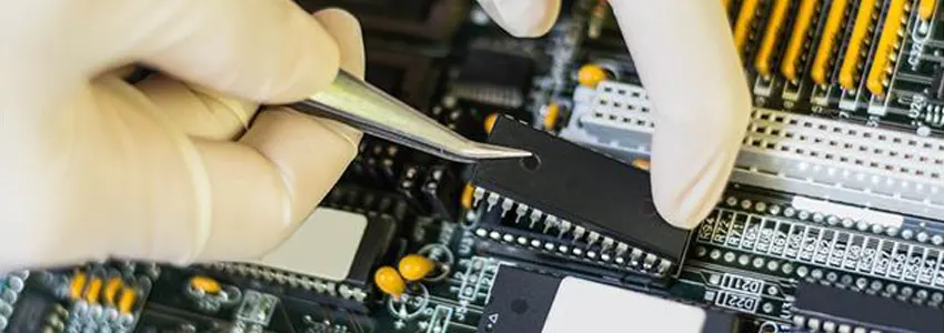
PCB assembly is the stage that follows the design and manufacturing phases of a customized printed circuit board project. Once the initial design work is completed according to client specifications, the builder proceeds to create the actual PCB boards. The next step involves sourcing and installing all the required ICs and other components, which is known as the assembly phase.
During this stage, the substrate and etched traces are prepared and ready for further progress. However, the PCB remains a mere slab of untapped potential until all the necessary parts are acquired and soldered onto their designated locations. To fulfill its intended purpose, the PCB must be meticulously and accurately assembled, ensuring that all the essential components are securely attached in their respective positions across the circuit.
Today’s PCBs predominantly utilize surface mount technology (SMT). This method enables the integration of smaller components, arranged more closely together, enhancing production speed and reducing costs.
In this process, solder paste is applied to the PCB using a stencil. The components are then accurately positioned by pick-and-place machines, following an operator’s inspection. The assembled PCB undergoes heating in an oven through reflow soldering, where the paste melts to firmly attach each component.
Through-hole PCB assembly, an older yet still relevant technique compared to SMT, is employed for specific applications. It involves drilling holes into the PCB for inserting component leads, resulting in more robust connections and enhanced product durability.
In the through-hole process, the leads of components are inserted into these pre-drilled holes, considering their specific position and polarity. After verifying the correct placement, an assembler uses heated solder paste to secure the components. The solder then cools and solidifies, forming a strong bond. Previously a manual process, advancements in technology have now enabled partial automation in both the soldering and assembly phases of through-hole manufacturing.
Mixed technology assembly combines various techniques, crucial for assembling single and double-sided PCBs. For single-sided mixed assembly, essential steps include solder paste printing, placement of surface-mounted device (SMD) parts, and reflow soldering. Additionally, wave soldering and through-hole technology (THT) placement are integral to the process. When it comes to double-sided mixed assembly, the process accommodates both adhesive-based and non-adhesive methods. Surface mount adhesive, though optional, may be employed depending on specific requirements. This approach incorporates all the steps used in single-sided assembly and adds procedures relevant to handling both sides of the PCB.
Achieving optimal outcomes in mixed technology assembly necessitates a harmonious integration of surface mount technology (SMT) and through-hole technology (THT). The process begins with the application of surface mount adhesive, followed by the precise placement of SMD parts. The assembly then undergoes a flipping process for alignment, leading to the solidification phase. Post solidification, wave soldering is conducted, concluding with the placement of components using PTH (Plated Through Hole) technology. This blend of SMT and THT ensures a comprehensive and effective assembly of PCBs, catering to a wide range of electronic applications.
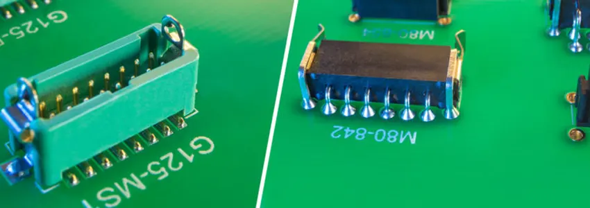
Surface Mount Technology (SMT) and Through-Hole Technology (THT) are two distinct methods used in PCB assembly. SMT involves directly soldering components onto the surface of the board’s substrate. In contrast, THT involves inserting the conductive leads of components through small holes in the substrate, and then soldering them on the opposite side of the board.
SMT is generally chosen for projects where strong mechanical bonds are less critical. It offers a quicker assembly process, further streamlined by employing Pick And Place machines for precise component arrangement before soldering. Components for SMT are typically smaller and less expensive, making this method more fitting for projects where cost-effectiveness and compact design are priorities, allowing for denser component placement.
On the other hand, THT is preferred when durable physical connections at solder points are necessary. This method is especially beneficial for certain types of connectors and hardware that demand robust attachment, depending on their use. THT assembly tends to be more time-consuming, as it involves extra steps in both the design and manufacturing stages. Soldering in THT can be done manually or semi-automated using Insertion Mount Machines.
Components for THT are usually larger and slightly more costly than their SMT counterparts, partly due to the need for conductive leads that can be inserted through the PCB. This structural requirement contributes to the differences in size and price between THT and SMT components.
We offer comprehensive turnkey PCB assembly services that encompass the entire process. This includes the manufacturing of Printed Circuit Boards, sourcing components, order tracking, ongoing quality monitoring, and final assembly.
● Full Turnkey PCB Assembly: We handle every aspect of the process, from PCB fabrication and parts procurement to order tracking, quality inspections, and final assembly. This comprehensive solution ensures a smooth and efficient process, ideal for projects requiring minimal involvement on your part.
● Partial Turnkey PCB Assembly: This option allows you to provide certain components (a partial list) while we handle the remaining procurement, assembly, and quality control. This approach offers flexibility for projects where you have specific sourcing requirements.
● Quick Turn PCB Assembly: We specialize in rapid prototyping and low-volume electronics manufacturing, ensuring timely delivery of your assembled PCBs. This service is ideal for projects with tight deadlines or requiring early-stage testing and validation.
● Prototype PCB Assembly: Our cost-effective prototype assembly service utilizes our turn-key expertise to provide a convenient and efficient solution for validating your PCB designs. We understand the importance of speed and accuracy during the prototyping stage.
● Low Volume PCB Assembly: We offer short-run production with our factory is located in China to provide the most competitive pricing for your small-scale projects. Low volume typically refers to quantities less than 1,000 PCBs.
● High Volume PCB Assembly: We cater to large-scale production requirements with our high-volume assembly services. We leverage our expertise and efficient processes to ensure top quality, rapid turnaround, and competitive pricing for your high-volume projects (typically exceeding 1,000 PCBs).
Our skilled technicians and advanced equipment ensure high-quality results, regardless of the size or complexity of your project.
● Surface Mount (SMT)
● Thru-hole
● Mixed Technology (SMT/Thru-hole)
● Single or Double Sided Placement
● Quickturn (1-5 days)
● Standard (10 days)
● Scheduled Deliveries
● No Minimum Order Requirement
● First Article Production
● From Prototype to Full Production
● Leaded
● Lead-free/RoHS Compliant
● No-clean and Water Clean Flux Options
● Passive Components as small as 01005
● Ball Grid Array (BGA)
● Quad Flat Package No-Lead (QFN)
● Quad Flat Package (QFP)
● Small Chip Packages (Minimum pitch of 0.2 mm)
● Rework Services
● Wire & Cable Harness Assembly
● Box Build Assembly
● Design for Manufacturability (DFM) Analysis
● X-Ray Inspection
● Aqueous Cleaning Processes
● PCB Testing Services
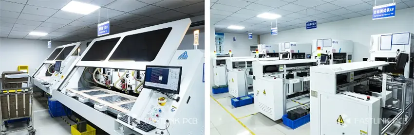
Our 65,000-square-foot state-of-the-art facility in Shenzhen houses the advanced equipment for manufacturing and assembling printed circuit boards. Fastlink leads the industry in quality and performance, whether you need standard fast PCBs or metal PCBs with tight tolerances.
There are more pictures of our factory’s equipment display in our company profile, please click here.
Our rigorous quality control process ensures that every PCB assembly, regardless of size or complexity, meets the highest standards. We conduct in-house testing, including ICT, X-ray, functional testing, and AOI, to deliver mass production in a cost-effective manner. Our lead times range from 1-5 days for standard projects and 1-2 weeks for complex projects, but we can expedite production for urgent orders. Whether you require low-volume prototypes, high-volume production runs exceeding 10,000 pieces, or anything in between, we can handle all your PCB assembly needs.
Choose Fastlink as your trusted partner for all your PCB assembly needs. Our comprehensive capabilities, commitment to quality, and dedication to customer satisfaction ensure a successful outcome for every project.