- [email protected] Mon-Sun 0. 00-23. 59
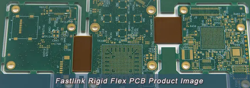
Rigid-flex circuit boards amalgamate the advantages inherent in both rigid and flexible circuit technologies, making them apt for portable devices. The flexible circuit segment adeptly conforms to required bends, enhancing design versatility, while the rigid circuit segment imparts stability and robustness to those areas demanding heightened durability and shock resistance.
Our custom-tailored flex and rigid-flex circuit board solutions cater to numerous prestigious OEMs. Fastlink holds a leading position in the industry in terms of both quality and delivery timelines. Our manufactured flexible circuits exhibit solid reliability, meeting the stringent requirements of aerospace, medical, and military domains. Serving as a high-reliability substitute for wire and wire harness assemblies, flex circuits deliver a notable cost reduction without compromising performance.
Rigid-flex PCBs amalgamate both flexible and rigid board technologies to suit specific applications. Typically, these boards comprise multiple layers of flexible circuit substrates affixed to one or more rigid boards either externally, internally, or both, contingent on the application design. The flexible substrates are engineered to remain in a perpetual state of flex, often being shaped into the requisite flexed curve during the manufacturing or installation phase.
The design process of Rigid-Flex boards presents a more intricate challenge compared to traditional rigid boards, given the three-dimensional design space they inhabit. This 3D design realm not only enhances spatial efficiency but also empowers designers with the liberty to twist, fold, and roll the flexible board substrates to attain the desired form, aligning with the final application’s packaging requisites.
A flexible PCB is a unique type of printed circuit board engineered to adapt to the specific contours of a product or system, thanks to its design made from thin, pliable material. These flex circuits exhibit a spectrum of complexity, ranging from a straightforward single-layer circuit to more intricate multilayer printed wiring circuit boards that comprise three or more conductive copper layers, usually featuring plated through holes.
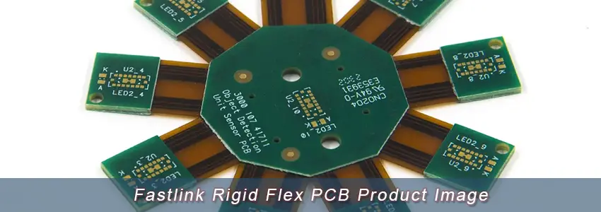
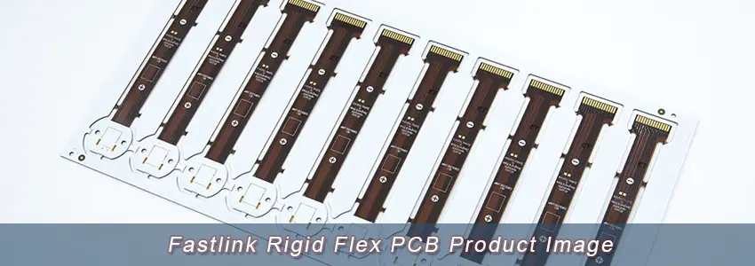
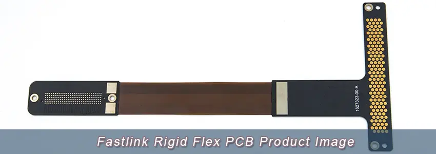
A rigid-flex circuit board emerges as a 3D interconnect capable of being bent and folded to conform to nearly any geometrical configuration. The advent of rigid-flex technology empowers designers to consolidate multiple PCBs interconnected by wires and/or cables into a singular unit, thereby enhancing performance while bolstering reliability. Rigid-flex circuits can burgeon up to 50 layers, supplanting cumbersome wire harnesses with a compact yet sturdy design.
The employment of rigid-flex circuit board technology significantly diminishes the requisite for bulky, weighty wire harness cables within an electronic ensemble. This not only economizes on installation time and component costs but also yields a neater and typically more compact top-tier assembly.
In numerous scenarios, traditional rigid circuit boards fall short in meeting the design exigencies of many portable devices. Although rigid boards lend a degree of shock resistance and strength to the device along with EMI/RF shielding, they often entail numerous points of interconnect to realize all necessary connections. Such interconnect points might encompass connector solder joints, connector-to-connector interfaces, wire solder joints, and crimped wire contacts among others. This proliferation of interconnect points elevates the likelihood of potential failure zones.
Furthermore, the connectors occupy valuable space within the portable device, potentially increasing its weight beyond desirable limits. The device packaging may need to be upscaled to house the rigid board, a modification that may not resonate well with customer preferences. A fundamental drawback of rigid boards is their inability to bend and flex to conform to curved device architectures or those necessitating flexibility.
Conversely, flexible circuit boards exhibit an aptitude for applications in portable electronics demanding bending and flexing capabilities. Their slender profiles allow for seamless integration around operational mechanisms without obstructing their functionality. Moreover, their lightweight nature suits applications where weight considerations are crucial for ensuring safe and reliable product operation.
Nonetheless, flexible circuits also necessitate connectors and the associated solder joints for interfacing with rigid circuits. This requirement retains the space consumption issue within the final assembly and does not notably diminish the requisite points of interconnect. Hence, while flexible circuits ameliorate some challenges posed by rigid boards, they introduce their own set of considerations that require thoughtful deliberation during the design phase.
1. Space and Weight Savings: Rigid-flex PCBs allow for more compact and lightweight design solutions. By eliminating connectors and replacing them with flex circuits, you can reduce the space and weight of the assembly, which is particularly beneficial in aerospace, automotive, and portable electronic applications.
2. Increased Reliability and Durability: With fewer connectors and solder joints, the potential points of failure are significantly reduced. The flexible portions can also absorb shocks and vibrations, enhancing the durability and reliability of the entire system.
3. Improved Electrical Performance: Rigid-Flex PCBs can provide excellent electrical performance. The shorter interconnect paths can result in lower impedance and less signal loss, beneficial in high-speed circuit designs.
4. Enhanced Design Flexibility: The 3D design capability enables complex geometric configurations, providing designers with a great degree of freedom to meet intricate design requirements. This is especially advantageous in modern electronics where unconventional form factors are often sought.
5. Optimized Packaging: By conforming to a variety of shapes, Rigid-Flex PCBs enable optimized packaging solutions. They can be folded or twisted to fit into tight spaces, ensuring that the PCB conforms to the package rather than dictating the package design.
6. Reduced Testing Complexity: With a simplified design and fewer interconnects, testing complexity is reduced, which can lead to faster and more efficient testing processes, ensuring a quicker time to market.
7. Environmental Resistance: The inherent design of Rigid-Flex PCBs lends itself well to resisting harsh environmental conditions, making them suitable for a wide range of industrial, aerospace, and military applications.
8. Integrated Rigid and Flexible Zones: The integrated design allows for rigid zones to house complex circuitry, components, and provide structural rigidity, while the flexible zones provide the necessary flexibility for dynamic applications.
9.Improved Thermal Management: The flexible layers can dissipate heat more effectively than traditional rigid boards, contributing to better thermal management within the system.
The design process of Rigid Flex PCBs is notably more intricate given their 3D design capability, which enables the board to be folded or twisted to attain the requisite shape for the product. Employing a 3D design approach not only amplifies spatial efficiency but also caters to unique scenarios where space and weight reduction are pivotal, such as in medical devices. The three-dimensional design realm permits designers to twist, fold, and roll the flexible board substrates to realize the desired form for the final application’s packaging.
Typically, Rigid Flex PCBs are leaner compared to other boards, making them a viable choice for products with slender or lightweight packaging requirements. With thin copper layers and adhesive-less laminates, they present a compact, thin, and light solution for circuit design endeavors.
Initially, the production process commences with the design and layout phase. During this phase, engineers leverage specialized PCB design software to craft a 3D model of the Rigid-Flex PCB, meticulously defining the layout, layers, and connections to ensure a coherent design. This software aids in visualizing how the rigid and flexible sections will interact. Following the design creation, a rigorous design review is undertaken to ascertain that the design meets the necessary specifications and standards, which include adherence to the IPC-2223 guidelines for Rigid-Flex PCBs. This step is crucial for preempting any design issues that could potentially arise during manufacturing.
Material selection is a pivotal step in the production process. It involves choosing suitable substrate and coverlay materials for both the flexible and rigid sections of the PCB. Common materials include polyimide for the flexible areas and FR4 for the rigid areas. The materials are selected based on various factors including their electrical, mechanical, and thermal properties to ensure they can withstand the operational demands of the final application.
Photolithography is a process employed to transfer the circuit pattern onto the material substrate. Initially, a light-sensitive photoresist material is applied to the substrate. Subsequently, the panel is exposed to UV light through a mask which outlines the circuit pattern. The unexposed areas are then developed away, leaving behind the desired circuit pattern on the substrate. This process is vital for achieving precise circuitry layouts on the PCB.
Following photolithography, etching is carried out to remove the exposed copper that is not protected by photoresist, leaving behind the desired circuitry. Etching ensures the accurate formation of circuit tracks, which is crucial for the electrical functionality of the PCB.
Drilling is performed to create holes for through-hole components and vias. Post drilling, an electroless plating process is conducted wherein a thin layer of copper is chemically deposited in the holes to prepare them for electroplating. This step is crucial for ensuring good connectivity between different layers of the PCB.
Electroplating is carried out to further plate the holes with copper, ensuring robust electrical connections. This process also enhances the thickness of copper on the circuitry to the specified level, facilitating better conductivity and long-term reliability.
Lamination is a critical step where the layers of the Rigid-Flex PCB are bonded together under heat and pressure. This process includes adhering the flexible and rigid layers together either with adhesive or directly through thermal bonding, ensuring a unified and robust structure.
The boards are then profiled to the desired shape and size through mechanical routing, and the flex areas are die-cut to ensure accurate dimensions. This step is essential for ensuring the PCB fits precisely into the intended assembly.
Component assembly begins with the application of solder paste to the board through a stencil. Automated machinery is then used in a pick-and-place process to position components onto the board. Following component placement, the boards are passed through a reflow oven to melt the solder and establish solid electrical connections between the components and the board.
Inspection and testing are paramount to ensuring the quality and functionality of the Rigid-Flex PCB. Automated Optical Inspection (AOI) and X-Ray Inspection are employed to check for soldering defects, alignment issues, and internal layer registration. Additionally, functional testing is carried out to ensure the board operates as per the design specifications.
Final finishing involves the application of surface finishes such as ENIG (Electroless Nickel Immersion Gold) or HASL (Hot Air Solder Leveling) to protect the board and provide a solderable surface. This step also enhances the board’s durability and solderability.
Lastly, the boards are meticulously cleaned to remove any residues, inspected once more for any defects, and then packaged securely for delivery. This final step ensures that the Rigid-Flex PCBs are delivered to the client in pristine condition, ready for integration into the respective applications.
Rigid Flex PCBs offer a unique blend of the mechanical stability of rigid PCBs and the flexibility of flex PCBs, making them suitable for a diverse range of application areas.
1. Aerospace and Defense: Rigid Flex PCBs are indispensable in aerospace and defense applications due to their lightweight, reliability, and space-saving attributes. They are used in satellite systems, avionics controls, missile guidance systems, and other military-grade electronics.
2. Medical Devices: In the medical sector, Rigid Flex PCBs find applications in wearable devices, medical imaging systems, and various diagnostic equipment. Their flexibility and compact design are well-suited for devices like pacemakers, hearing aids, and other wearable monitoring systems.
3. Consumer Electronics: The demand for sleek, compact, and highly reliable devices in consumer electronics propels the use of Rigid Flex PCBs. They are utilized in smartphones, tablets, laptops, wearables, and other portable electronic devices.
4. Telecommunications: Rigid Flex PCBs are employed in various telecommunications equipment including routers, switches, and high-speed servers due to their ability to maintain signal integrity over flex regions.
5. Automotive Industry: The automotive sector leverages Rigid Flex PCBs in applications like control systems, entertainment systems, GPS, and other electronics within vehicles. Their durability under harsh conditions and ability to save space makes them apt for modern automotive electronics.
6. Industrial Controls: In industrial control systems, Rigid Flex PCBs are utilized for their robustness, and ability to withstand harsh industrial environments. They are found in automation equipment, monitoring systems, and other industrial electronics.
7. Testing Equipment: Rigid Flex PCBs are chosen for various testing and monitoring equipment due to their reliability and precise performance under varying conditions.
8. Semiconductor: In the semiconductor industry, Rigid Flex PCBs find applications in test fixtures and other equipment used in the manufacturing and testing of semiconductor devices.
| Number of Layers | 4-18 Layers |
| Build Time | 1-2 Weeks |
| Polyimide Base Material | Polyimide(PI), PET, Polyester-Flex |
| Rigid Base Materials | Rogers, ISOLA, Nelco, Taconic, Shengyi etc. |
| FPC Thickness | 0.1 – 0.6MM |
| Rigid Thickness | 0.4 – 5.4MM |
| Min Track / Spacing | 3Mil/Mil |
| Min Hole Size (diameter) | 0.1MM-0.2MM |
| Coverlay (Flex Part) | Yellow Coverlay, White Coverlay, Black Coverlay |
| Silkscreen Color | Yellow, Red, White, Black, Etc. |
| Surface Finish | Plated Gold, Immersion Gold, OSP, Immersion Silver, Immersion Tin, etc. |
| Finished Copper | 0.5 oz – 6 oz |
| Stiffener Material | FR4, Steel, Aluminum and PI |
Fastlink has provided quality rigid-flex PCB manufacturing services to companies in a variety of industries including medical, telecommunications and manufacturing. We house a dedicated quality control department to ascertain the precise fabrication and assembly of your boards – furthermore, we assure the quality of all parts and components.
The utilization of a 3D engineering environment enables us to attain spatial efficiency and incorporate essential folds and flexes to align with the desired shape optimal for your application.
Regardless of the requirement for a basic flexible PCB or a sophisticated multilayer rigid-flex solution, Fastlink is able to manufacture and assemble the highest quality Flexible, Rigid-Flex and HDI Flexible Printed Circuit Boards in China.
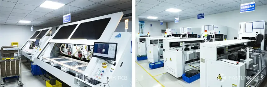
Our 65,000-square-foot state-of-the-art facility in Shenzhen houses the advanced equipment for manufacturing and assembling printed circuit boards. Fastlink leads the industry in quality and performance, whether you need standard fast PCBs or metal PCBs with tight tolerances.
There are more pictures of our factory’s equipment display in our company profile, please click here.
We are duly certified with the following accreditations:
● IATF 16949:2016
● ISO 9001:2015
● ISO14001:2015
● ISO13485:2016
● UL
Furthermore, all our products adhere to the IPC & ROHS Standards. It is our continuous endeavor to produce premium quality PCB products.