- [email protected] Mon-Sun 0. 00-23. 59
With the advancement of technology in the medical field, diagnostics and treatments increasingly rely on automated machinery. These machines, in turn, rely on PCBs. PCBs are compact assemblies of intricate circuits that accommodate a multitude of components within a small space. The PCB assembly typically incorporates several advanced features to ensure the precision and reliability of the product.
Fastlink offers design and engineering assistance for producing a wide range of medical PCB prototypes, from small-scale testing to large-scale production. Additionally, we provide comprehensive support for the assembly, integration, and testing of medical PCBs. This not only expedites the launch of cutting-edge medical products but also ensures compliance with rigorous medical PCB standards by maintaining strict control over processes, quality, and traceability.
In the realm of electro-medical devices, mirroring trends in other electronics sectors, there’s a shift towards producing smaller products packed with a higher density of components. This evolution impacts the design of PCBs in several ways, including component layout, spacing, trace length and separation, and PCB heat dissipation. Consequently, the margin for error in PCB design has significantly reduced, demanding more adaptability in both the design and manufacturing stages.
A pivotal technology in addressing these challenges is the HDI PCB. HDI technology facilitates the creation of compact PCBs while accommodating an increasing number and complexity of functions. This advancement leads to a reduced space for trace routing, where traces are positioned more closely.
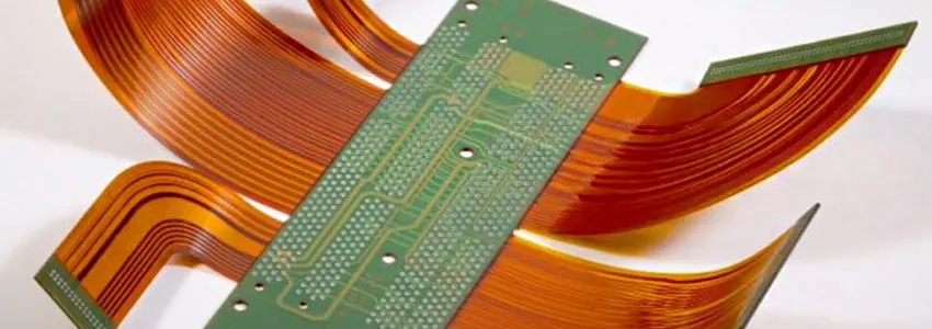
Another prominent technology in medical PCBs is the use of flex and rigid-flex boards. These boards are particularly suited for medical devices that require deviation from the standard dimensions and shapes of traditional PCBs. Their use is crucial for fitting into smaller spaces while maintaining the necessary reliability and durability. Flex PCBs are lighter, contributing to a reduction in the overall weight of the device. Their flexibility also enhances space utilization and lowers manufacturing costs, providing designers with more freedom in choosing the device’s form.
The design process for flexible PCBs, while more complex than for rigid ones, streamlines the creation of ergonomic and robust medical devices. In wearable applications, flexible PCBs offer significant mechanical advantages over their rigid counterparts. Additionally, they can be connected to rigid boards using thin flat cables. This feature allows for a seamless integration without the need for bulky connectors, further optimizing the design and functionality of medical devices.
The design of medical PCBs is a demanding process that hinges on a deep comprehension of electrical properties and circuit theory. This knowledge is crucial for creating a board that not only functions accurately but also adheres to critical safety standards. In the realm of medical devices, the electromagnetic compatibility (EMC) of PCBs is of paramount importance. Any interference or perturbation in electrical signals can lead to diagnostic inaccuracies or malfunctions in medical equipment, which are unacceptable risks.
These circuit boards typically incorporate various components such as integrated circuits, resistors, and capacitors, alongside other packaging elements. Modern medical PCB designs often employ SMT and may integrate flexible printed circuit boards (Flex PCBs). These designs must also take into account environmental resilience and safety considerations, including factors like temperature stability and shock resistance.
Crafting a medical PCB is a sophisticated and intricate task, demanding not only knowledge and experience but also a high level of precision. Designers must have a thorough grasp of electrical properties and circuit theory to create designs that are both reliable and robust. It is essential to consider safety and environmental factors in these designs to ensure user protection. The role of medical PCB design in the development of medical devices is crucial. It is the cornerstone that guarantees these devices’ reliability, safety, and regulatory compliance.
The process of creating medical-grade PCBs shares several similarities with the fabrication of standard PCBs, with some distinct variations in certain stages like imaging and etching.
In the production of regular PCBs, a subtractive etching method is commonly used. This involves coating the copper foil with a photoresist, which is then exposed to UV light through a negative image of the circuit pattern. The areas exposed to UV light harden, defining where the circuit pattern Ais needed. The etching solution then removes the superfluous photoresist and the underlying copper, leaving behind the copper in the pattern of the circuit.
A notable limitation of this subtractive etching approach is the formation of non-uniform tracks. As the etching process erodes copper from the top, the track walls take on a trapezoidal shape rather than being vertical. This results in variable track widths and difficulties in achieving fine spacing.
For medical-grade PCBs, which demand precise control over thin tracks and fine spacing, a modified semi-additive process (mSAP) is employed. This begins with the electrolytic thinning of the copper on a copper-clad laminate until a very slim layer remains. The desired circuit pattern is then imprinted onto this thin layer using laser direct imaging, exposing the necessary copper paths.
The fabricator subsequently adds a thick layer of electrolytic copper onto these exposed areas. After achieving the required thickness, they remove the excess resist chemically and etch away the unwanted copper. Since this method involves adding copper instead of removing it, it’s considered an additive process.
The benefit of this additive approach lies in its ability to produce very thin tracks with precise spacing, thanks to the vertical walls of the tracks. Additionally, the electrical deposition of copper on a laser-defined image allows for much tighter control over track width, crucial for the high standards required in medical-grade PCBs.
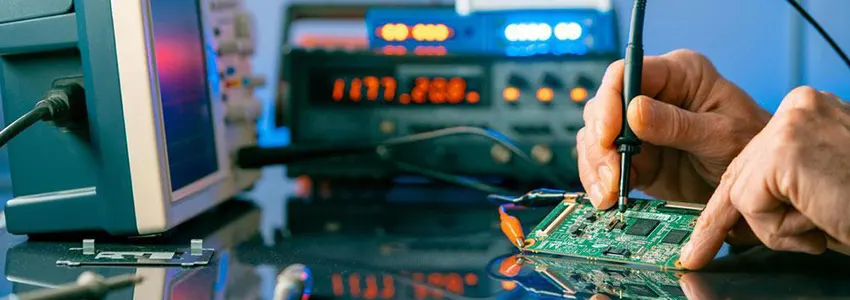
Once the PCB design and fabrication are completed, the next critical phase is its assembly. In this stage, various electronic components are soldered onto the board. This step transforms the PCB from a mere fabricated structure into a functional unit, capable of performing its designated tasks. Without the assembly of components, the fabricated PCB cannot fulfill its intended function.
Before commencing the PCB assembly, several key factors must be taken into account. These include the type of circuit board, the attributes of the PCB components, and the overall function of the board. Preparation for assembly also involves gathering essential tools and materials. Necessary equipment includes testing apparatus, soldering machines, and SMT equipment. Additionally, materials like solder wire and solder paste are indispensable for the process.
Given the critical nature of applications in the medical sector, it’s crucial to conduct a Design for Manufacturability (DFM) test before the assembly begins. The DFM test aims to detect and rectify any potential design issues, ensuring the final medical board operates as intended. This pre-assembly evaluation is vital to guarantee that the finished medical PCB meets all requirements and functions correctly in its medical applications.
The final phase in the assembly of Medical PCBs involves a detailed inspection and testing of the completed board. This critical step ensures that the board functions correctly and adheres to the stringent standards of the medical industry. After the board passes these tests and is deemed suitable, it undergoes a thorough cleaning process. This step involves washing the board to eliminate any residues like oil, flux, or dirt, rendering it pristine and appropriate for integration into medical devices. Additionally, based on the specific type of medical equipment that will incorporate the Medical PCB, specialized tests may be conducted on the board to confirm its suitability for the intended application.
Fastlink is a reliable partner and comprehensive provider for PCB fabrication, component sourcing, PCB assembly, and electronic manufacturing services. Boasting over a decade of experience, we have successfully supplied high-quality PCBs at competitive prices to over a thousand customers across the globe. Our company holds ISO9001:2015 Certification and is UL Listed. We guarantee quality through 100% E-testing and inspections using both AOI and X-RAY techniques, ensuring the provision of products that comply with industry standards. Contact us today to get a fast quote.