- [email protected] Mon-Sun 0. 00-23. 59
The telecommunication industry relies on integrated circuitry within PCB designs to enhance signal integrity and optimize transmission. These circuits are intricately designed to reduce noise, boost network efficiency, and facilitate smooth data exchange. They play a pivotal role in the consistent and efficient transmission of voice, video, and data signals. This efficiency is achieved by employing advanced methods such as impedance management and signal conditioning, crucial for the evolution of high-speed communication networks.
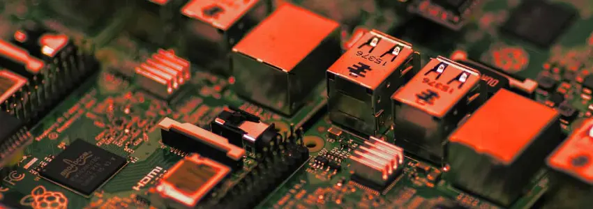
Our company provides high-reliability, high-performance communication PCBs that maintain signal integrity throughout their lifespan, ensuring no delay or latency in transmission. We address impedance challenges and incorporate various via structures like blind, buried, or micro vias to meet device miniaturization needs. Depending on the specific requirements of the device, we offer an array of fabrication solutions including HDI, Rigid, Flex, and Rigid-Flex. Adhering to stringent quality standards, we perform multiple automated tests and inspections to guarantee the delivery of top-quality products.
Communication PCB refers to a printed circuit board specifically designed for communication applications. PCBs are fundamental components in modern electronics, used to mechanically support and electrically connect electronic components using conductive pathways, or traces, etched from copper sheets laminated onto a non-conductive substrate.
In the context of communication, these PCBs are tailored for devices and systems that facilitate communication, such as smartphones, radios, routers, and other telecommunications equipment. Here are some key aspects of communication PCBs:
1. High-Frequency Operation: Communication devices often operate at high frequencies (e.g., GHz range for wireless communication), so the PCBs are designed to handle these frequencies with minimal signal loss or interference.
2. Impedance Control: Critical for maintaining signal integrity in high-speed communication.
3. Thermal Management: Communication devices can generate significant heat, so these PCBs often incorporate features for better heat dissipation.
4. Multiple Layers: Communication PCBs have multiple layers to accommodate the complex circuitry required for sophisticated communication technologies.
5. Reliability and Durability: These PCBs are often designed to be highly reliable and durable, as communication devices are essential in many critical applications.
6. Integration of Various Technologies: They integrate various technologies, such as RF (Radio Frequency) and microwave components, to support a range of communication standards.
7. Miniaturization: As communication devices tend to get smaller, the PCBs also need to be compact yet highly functional.
When selecting a PCB for the telecommunications industry, it’s important to tailor the choice to the specific application. In office communication environments, PCBs are integral to video collaboration systems, phone switching systems, PBX systems, and VOIP devices. Meanwhile, broader telecommunications infrastructure relies on PCBs for cell towers, high-speed routers, satellite systems, servers, and commercial phones. Additionally, telecommunication PCBs are vital for LED display control and indicators.
Different telecommunication applications demand distinct types of PCBs. Many of these applications are situated outdoors and thus require PCBs that can endure tough environmental conditions, including extreme weather and harsh climates. For these situations, temperature-resistant and highly durable PCBs are essential.
Fastlink is equipped to provide a diverse range of printed circuit boards tailored to meet the needs of all telecommunication applications.
Communication devices depend on PCBs to provide strong and consistent connectivity for intricate, high-speed components. It’s crucial to maintain signal integrity as signals are transmitted between transceivers, antennas, power amplifiers, and more.
Communication device signals often operate at high frequencies, particularly in the microwave band. For instance, smartphones use multiband antennas compatible with 4G and 5G frequencies – ranging from 700 MHz to 5 GHz in newer generations. This demands PCBs made with materials and construction techniques that support efficient signal transmission, minimizing issues like dielectric power loss or RF conduction path leakage. We select substrates and lamination materials designed for high-frequency use, considering factors like dielectric constant, loss tangent, thermal conductivity, and TCE.
Beyond frequency, the capacity for high data rate throughput is critical. Modern phones, with multi-Gbps Wi-Fi 6 speeds and high-bandwidth wireless interfaces, require PCBs with finely spaced traces (commonly 4-6 mil line/space for data lines). Managing short, closely routed signal paths calls for low-loss, tight impedance tolerance laminates and precise stackups for characteristic impedance control. Designing the number of layers, trace dimensions, dielectrics, and laminate materials is vital to preserve signal integrity in these high-speed paths.
Communication PCBs require effective measures to prevent unwanted coupling between traces due to the presence of complex components in close proximity and high-frequency interactions. To achieve this, our engineers employ various techniques, including ensuring short signal return paths, utilizing reference planes, and employing strategic component placement to facilitate field confinement. Additionally, we prioritize stackup symmetry, implement selective isolation and shielding around sensitive components, incorporate ground stitching vias alongside traces, and apply specialized treatments. These measures effectively eliminate EMI emission and minimize crosstalk in densely designed layouts that feature high-speed traces across multilayer boards.
Selecting the right materials for PCBs in communication products is a crucial step. It involves choosing suitable substrate laminates, prepregs, conductive layers, coatings, and finishes to meet the electrical, mechanical, and environmental demands of these applications.
FR-4, a glass-reinforced epoxy, is a standard PCB substrate. It provides reliable electrical insulation, mechanical strength, and environmental resilience at an affordable cost. We source high-quality FR-4 cores and prepregs from top Asian suppliers. Our stable partnerships guarantee a consistent supply of materials that meet both IPC standards and our rigorous quality control requirements.
For systems operating above 1GHz, low-loss circuit board dielectrics are essential. We provide a variety of high-frequency/low-loss laminates, such as Rogers RO4000, RO3000, RT/duroid series, Isola, and Taconic TLY and TFLY families for microwave applications. We carefully select materials based on dielectric constant and loss tangent to achieve optimal impedance matching, ensuring signal integrity at the desired frequencies and data rates. These materials undergo thorough testing to confirm their modeled electrical performance.
In environments that demand extreme tolerance and stability at microwave frequencies, ceramic-filled PTFE substrates like Rogers’ RT/duroid 6202PR excel. They are particularly suited for applications with severe thermal cycling and corrosive conditions, such as in avionics. The dimensionally stable PTFE matrix with low Dk ceramic filler is ideal for creating 2.5D glass microvia interconnects, which are crucial for high-frequency front-end modules.
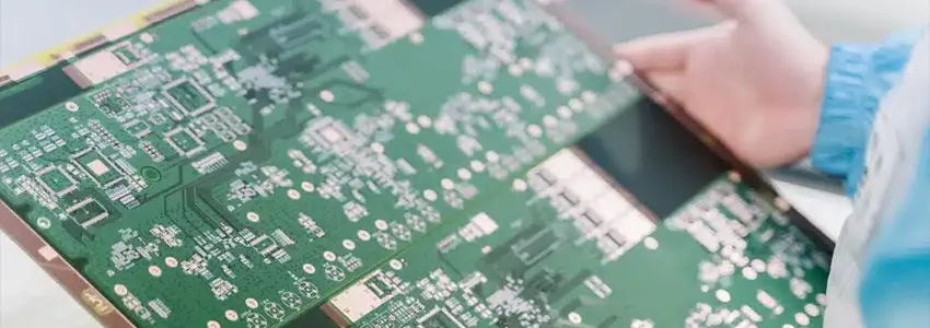
In our production of telecom PCBs, we ensure precise component placement, advanced manufacturing techniques, and strict adherence to industry standards for signal integrity. We perform thorough testing and inspections to ensure our PCBs comply with all essential requirements and standards, a crucial step for the effectiveness of communication systems.
We provide reliable PCB solutions that effectively meet the stringent requirements of high-speed and high-frequency communication systems. To meet the demands of RF and baseband components, we employ advanced materials, such as ceramic substrates, when necessary.
With our seasoned engineers and cutting-edge facilities, we have the capability to handle the intricate design and processing demands associated with communication PCBs. We are proficient in fabricating multi-layered PCBs with both precision and efficiency. This includes implementing through-hole plating and back-drilling techniques, which are pivotal in maintaining outstanding signal integrity and reducing signal reflection.