- [email protected] Mon-Sun 0. 00-23. 59
When incorporating printed circuit boards (PCBs) into your projects, their performance and reliability are paramount. To guarantee client satisfaction, a robust PCB testing method is crucial.
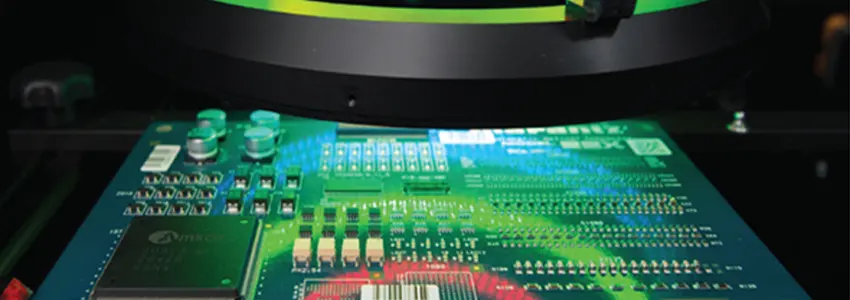
Automated optical inspection (AOI) is an indispensable process in PCB fabrication and assembly, effectively identifying defects and ensuring PCB functionality. This technology plays a pivotal role in scrutinizing electronic assemblies and PCBs, guaranteeing high-quality products devoid of manufacturing faults.
If your goal is to develop a flawless PCB for your electronic device, from initial design to the final product, Fastlink offers an ideal Automated Optical Inspection solution tailored for your needs.
Despite significant advancements, modern circuits are far more intricate than their predecessors. The introduction of surface mount technology and subsequent size reductions have resulted in exceptionally compact boards. Even basic boards contain thousands of soldered joints, which are common sites for defects.
This heightened complexity renders manual inspection impractical. Even when it was considered viable, manual methods proved ineffective due to inspector fatigue and the potential for overlooked defects. The current market demands high-volume, high-quality products delivered rapidly, necessitating reliable and efficient methods to maintain product quality. AOI, or automated optical inspection, is an essential tool in integrated electronics testing strategies, ensuring cost-effectiveness by detecting faults early in the production line.
AOI systems can be integrated into the production line immediately following the soldering process, enabling early defect detection. This offers several advantages. Firstly, faults are less expensive to rectify when detected early. Secondly, soldering and assembly issues can be identified promptly, allowing for rapid feedback to earlier stages. This swift response ensures that problems are recognized and resolved before a significant number of boards are produced with the same defect.
Automated Optical Inspection (AOI) systems are composed of two primary components: an optical system and a specialized software algorithm, both tailored to the specific manufacturing process.
The optical system is central to an AOI system. It captures images of the item to be inspected, and the quality of these images is vital for the system’s overall effectiveness. Typically, an AOI optical system includes a light source, a series of lenses, and a digital camera.
● Light Source: Illuminates the product being inspected. Its type, color, and illumination angle significantly affect defect detection. While older systems utilized fluorescent or incandescent lamps, and even ultraviolet lights, modern systems predominantly use LED arrays or halogen lamps for consistent, uniform lighting.
● Lenses: These direct light reflected from the product into the camera sensor. Their quality is crucial for capturing clear images. The lens system is adjustable, allowing for different fields of view and depths of field, suitable for a variety of product sizes and types.
● Camera: This component captures the product’s image. AOI system cameras range from standard 2D cameras to advanced 3D sensors, gathering depth information. The camera’s pixels convert received light into digital data, which the AOI software then processes for inspection.
The AOI machine’s effectiveness heavily depends on its software algorithms. These algorithms analyze the data from the optical system, identifying defects or anomalies in the inspected items. They act as the AOI system’s ‘brain,’ distinguishing between acceptable units and those with defects.
Common software algorithms in AOI include:
● Pattern Matching Algorithms: These compare the inspected item’s image against a reference image to detect deviations. They are effective in scenarios where component placement and orientation consistency is crucial.
● Statistical Pattern Matching: An advanced form of pattern matching, this algorithm learns from variations in appearances of good units, using statistical measures to identify significant deviations.
● Feature-based Algorithms: Useful for complex inspections, these algorithms identify and measure specific image features (like edges, corners, colors, or textures) and compare them against set criteria.
● Machine Learning (ML) Algorithms: Increasingly popular, ML algorithms, often based on neural networks, are trained on numerous images to identify diverse and complex defect types. These are particularly useful for varying product appearances or complex defect patterns.
The choice of algorithm largely depends on the inspection task’s specifics, as certain algorithms may excel in some scenarios but not others. Selecting the most effective algorithm requires a deep understanding of the inspection requirements.
AOI plays a crucial role in identifying defects in Surface Mount Technology (SMT) and Wave soldering processes. Our proven technology can effectively inspect and detect a wide range of manufacturing errors.
AOI can detect a variety of defects, including:
● Billboarding
● Component offset
● Component polarity
● Component presence or absence
● Component skew
● Excessive solder joints
● Flipped components
● Height defects
● Insufficient paste around leads
● Insufficient solder joints
● Lifted leads
● Missing components
● Paste registration
● Severely damaged components
● Solder bridges
● Tombstoning
● Volume defects
● Incorrect components
● Bridging
The advent of SMT and other compact circuit boards has enabled the integration of powerful circuits into smaller devices, opening up a realm of unprecedented technological possibilities. However, this miniaturization has also introduced increased complexity into circuit board development. With thousands of soldered joints on an average-sized board, the potential for defects, such as missing components or flaws, is amplified.
The growing complexity of circuit boards renders manual inspection impractical. The sheer number of tightly packed components makes manual examination time-consuming and prone to errors due to inspector fatigue and the likelihood of overlooking defects.
With the continuous shrinking of components, the positional accuracy of both inspection equipment and manufacturing processes becomes increasingly crucial. As a rule of thumb, AOI systems should offer sub-pixel accuracy, ensuring sufficient precision to detect subtle positional deviations that could lead to 01005 defects.
AOI testing enhances PCB pass rates, thereby lowering PCB costs.
AOI testing effectively inspects both PCBs and PCB assemblies. For PCBs, it detects defects such as shorts, opens, and insufficient solder. For PCB assemblies, it scrutinizes component soldering, polarity, and values.
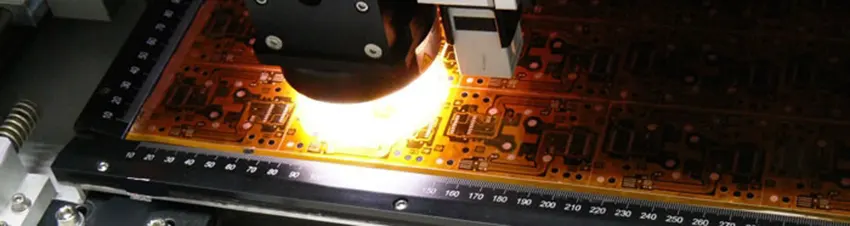
Lighting plays a critical role in achieving desired outcomes in machine vision applications. The ever-changing electronics fabrication environment necessitates dynamic lighting to ensure the widest defect coverage for various component and PCB configurations. Leveraging the cost-effectiveness of light-emitting diodes, AOI systems can configure highly customizable light arrays within the inspection software. Additionally, AOI systems can flexibly adjust image contrast, facilitating the identification of diverse defect conditions with multiple colors at different angles. Programmable lighting serves as an invaluable tool for maximizing defect detection capabilities.
Data collection and retrieval are essential functions of any AOI system. Data can be presented in various formats, including text output, image collection, databases, or combinations thereof. While data collection is a standard feature of most AOI systems, information retrieval is often more complex and depends on the configuration of the manufacturing line.
AOI can be integrated at any stage of the fabrication process, depending on specific needs and cost tolerance levels. Implementing AOI testing after reflow soldering is particularly beneficial as most defects arise from soldering process failures, reducing corresponding costs and enhancing inspection efficiency. Additionally, AOI enables immediate adjustments to fabrication or assembly parameters, ensuring the correct manufacturing of subsequent products.
AOI offers several advantages over other PCB defect detection methods. Here’s a comparison of AOI to alternative inspection techniques:
AXI utilizes X-rays, not light imaging, to inspect PCBs. Companies often employ AXI for evaluating highly complex or densely populated boards. X-rays penetrate materials to image them, whereas AOI’s light reflects off surfaces, potentially obscuring components. X-rays traverse various material layers, providing accurate images of all layers.
AXI’s primary drawback is its high cost. Due to its expense, AXI is typically reserved for exceptionally complex or densely populated boards.
ALT measurement employs lasers, not traditional light imaging, to scan and measure PCBs. As laser light reflects off PCB components, the ALT system uses laser positions to pinpoint component placement, height, and reflectivity. Similar to AOI, the ALT system compares empirical measurements to a schematic or specifications to detect flaws.
ALT measurement is particularly useful for evaluating solder paste location and quantity, but interference can sometimes cause inaccurate measurements.
ICT utilizes an electrical probe to assess the functionality of an assembled PCB. Electrical current is used to verify that each component is correctly positioned and functioning. It tests for shorts and open circuits and evaluates essential electrical properties like capacitance and resistance.
As it uses electrical current, ICT provides less detailed soldering information than AOI. It can evaluate electrical component quality and provide information about soldering defects affecting circuitry, but it offers limited detail on insufficient or excessive solder.
AOI is generally more reliable than ICT, especially for today’s smaller PCBs.
PCB companies often prefer AOI over MVI because AOI doesn’t require touching the boards. Manual inspection involves handling boards, which could introduce defects. AOI can scan PCBs without disturbing delicate components, preserving structural integrity.
AOI is also more reliable than MVI. Humans can easily miss minor PCB flaws. AOI detects even the smallest errors. Its precision never diminishes, it scans PCBs in finer detail than the human eye, and it consistently performs reliably throughout the production process.
Fastlink’s AOI solutions are quick, accurate, and efficient, ensuring your PCBs reach the manufacturing stage without rework or troubleshooting delays. We offers competitive pricing, providing significant cost savings for our clients. Find reliable Automated Optical Inspection (AOI) services in China, contact us today.