- [email protected] Mon-Sun 0. 00-23. 59
Ceramic PCB diverges from traditional fiberglass or epoxy resin usage, opting instead for a ceramic material as its foundational substrate. This specialized PCB encompasses a thin insulating layer constructed from ceramic material, amalgamated with metal components to formulate the circuitry. The ceramic base materials utilized in these PCBs, including alumina, aluminum nitride, or beryllium oxide, demonstrate outstanding heat conduction capabilities.
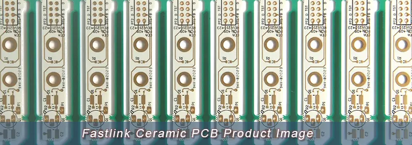
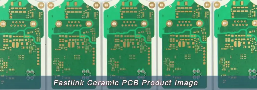
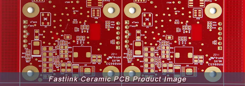
Fastlink, a Chinese manufacturer of ceramic PCBs, presents competitive pricing. We are fully equipped to meet your requirements for Ceramic PCBs and Ceramic Substrates, employing DPC (Direct Plating Copper) materials such as Aluminum Oxide (Al2O3) and Aluminum Nitride (AlN).
The trio of predominant ceramic materials employed in PCB manufacturing:
Alumina stands out due to its mechanical fortitude, chemical resilience, thermal conductivity, and electrical attributes when juxtaposed with other oxide ceramics. The plentiful availability of raw material catapults alumina to the forefront as the most prevalently utilized ceramic substrate material. Al2O3 ceramic PCBs find their applications in automobile sensor circuits, shock absorbers, and engines. The elevated thermal stability of Al2O3 ceramic PCBs augments the performance and thermal efficiency of the circuits deployed in automobiles.
Aluminum Nitride is heralded for its high thermal conductivity and coefficient of expansion, characteristics that render it a noteworthy substrate material within the PCB industry. The thermal conductivity of AlN oscillates between 170 W/mK to 220 W/mK. The Coefficient of Thermal Expansion (CTE) of AlN ceramic resonates with that of silicon semiconductor chips, fostering a robust bond between them and thereby enhancing the reliability of their assembly. AlN is employed in sensor circuits within automobiles, enduring extreme temperatures, corrosion, and vibration while delivering efficient, precise, and sensitive sensor signals.
Beryllium Oxide emerges as a ceramic PCB substrate material with a thermal conductivity nearly nine-fold that of Al2O3 and surpassing that of metallic aluminum. BeO exhibits superior chemical stability compared to AlN and high electrical isolation on par with Al2O3. It is utilized in scenarios where the PCB is subjected to elevated temperatures or in high-density PCBs constrained by space, rendering air or liquid cooling unfeasible.

1. High Thermal Conductivity: Ceramic materials inherently have high thermal conductivity, which allows for efficient heat dissipation. This property is especially beneficial in high-power or high-temperature applications where managing thermal loads is critical.
2. Low Coefficient of Thermal Expansion (CTE): Ceramics have a low coefficient of thermal expansion, which means they expand less when heated. This is crucial in electronics where differing expansion rates between materials can cause mechanical stress and potentially failure.
3. Excellent Electrical Insulation: Ceramic PCBs offer outstanding electrical insulation. They are capable of withstanding high voltages and provide excellent isolation between electrical components, which is crucial for the reliability and safety of electronic circuits.
4. Chemical Resistance: They are chemically stable and can withstand exposure to harsh chemicals without degradation. This makes them suitable for use in chemically harsh environments.
5. High Mechanical Strength: Ceramic materials are known for their high mechanical strength and rigidity, providing a robust platform for mounting heavy or sensitive components.
6. High Frequency Performance: Ceramic PCBs exhibit superior high-frequency performance due to their low dielectric constant and loss tangent. This makes them an excellent choice for RF (Radio Frequency) and microwave applications.
7. Long-Term Stability: They exhibit long-term stability under varying environmental conditions, making them reliable for use in a wide range of applications over extended periods.
8. Hermeticity: Ceramic PCBs can be hermetically sealed, which is beneficial in applications that require an airtight enclosure to protect sensitive electronics from environmental contaminants.
9. Fine Line Processing: The material properties of ceramics allow for fine line circuitry and higher resolution in the circuit design, which is advantageous in miniaturized and high-density circuit applications.
The categorization of ceramic PCB fabrication methodologies yields three distinct classifications: High-Temperature Co-fired Ceramic PCB, Low-Temperature Co-fired Ceramic PCB, and Thick Film Ceramic PCB.
High-temperature co-fired Ceramic (HTCC) substrates embody aluminum oxide cast ceramics infused with tungsten, molybdenum, and a blend of molybdenum and manganese. These constituents coalesce to form a metal-heating resistor paste endowed with a high melting point. This paste is meticulously imprinted upon 92-96% alumina green bodies, succeeded by lamination of 4-8% sintering aids across multiple strata. A co-firing procedure at temperatures scaling between 1500-1600°C engenders attributes like high-temperature resistance, corrosion resilience, extended lifespan, energy efficiency, uniform temperature distribution, and elevated thermal conductivity.
The fabrication of HTCC ceramic substrates unfolds through a nuanced and multistage process encompassing powder preparation, casting, slicing, punching, electrode printing, lamination, isostatic pressing, cutting, sintering, and plating.
HTCC-based PCBs are aptly suited for diverse applications, including ceramic heaters, infrared physiotherapy instruments, high-power micro-assembly circuits, and electronic packaging sectors. Their popularity stems from precision circuit interconnection facilitated by high thermal conductivity, robust insulation, and significant mechanical strength, all achieved through firing in high-temperature environments exceeding 1500°C.
Low-temperature co-fired Ceramic (LTCC) PCBs emerge from an assembly of multiple single-layer ceramic/glass/organic (green) sheets, subsequently perforated to form vias and screen printed with conductive, dielectric and resistive pastes to manifest circuit elements. Following a trimming process, these layers are fired at elevated temperatures, resulting in a sturdy substrate boasting exceptional dielectric properties, a low coefficient of thermal expansion, and superior thermal conductivity. Active and surface mount devices are then affixed atop the emitter stack, finalizing the multilayer electronic circuit.
LTCC PCBs thrive under extreme environmental conditions and exhibit a remarkable aptitude for high functional density and reliability, finding their niche in telecommunications, defense, and assorted domains. Their high density, reliability, and high-speed circuit board traits make them a favored choice among technology corporations. For example, in the United States, the Don Company employed an 8-layer, low-temperature co-fired multilayer substrate in the test circuit of the Stinger missile. In Japan, Fujitsu utilizes 61-layer low-temperature co-fired ceramic substrates for crafting multi-chip modules for VP2000 series supercomputers, while NEC produces 78-layer low-temperature co-fired multilayer substrates, sprawling over an area of 225*225 mm2, featuring 11540 I/O terminals with the capacity to house up to 100 VLSI chips.
Thick film ceramic PCBs are delineated by their conductor layer, which may span a thickness beyond 10 microns yet remain below 13 microns. Typically, the ceramic PCB surface is embellished with a conductor layer diligently imprinted using precious metals like silver or gold palladium. This entails the application of gold and dielectric pastes onto a ceramic base material, followed by a baking endeavor at temperatures sub-1000 degrees Celsius. Due to the relatively economical gold conductor paste, the adoption of thick film ceramic PCBs is prevalent among PCB manufacturers.
A cardinal advantage of thick film ceramic PCBs over traditional counterparts is their prowess in shielding copper from oxidation. This facet empowers ceramic PCB manufacturers to interlace interchangeable conductors, semiconductors, capacitors, and resistors on the ceramic board.
1. High-Power Electronics: Ceramic PCBs are ideal for high-power electronics due to their excellent thermal conductivity which facilitates efficient heat dissipation. This is critical in ensuring the reliability and extending the lifespan of power electronic devices such as power converters, inverters, and amplifiers.
2. LED Lighting: The high thermal conductivity of ceramic PCBs is advantageous in LED applications as it helps in managing the heat generated by LEDs efficiently. This is crucial in maintaining the performance and longevity of LED lights, especially in high-power LED lighting systems.
3. Automotive Electronics: Ceramic PCBs find applications in the automotive industry, particularly in power modules for electric and hybrid vehicles, sensors, and control units. Their low coefficient of thermal expansion (CTE), high thermal conductivity, and mechanical strength make them suitable for the harsh and demanding automotive environments.
4. Aerospace and Defense Electronics: The aerospace and defense sectors demand high-reliability electronics capable of withstanding harsh environments. Ceramic PCBs’ resistance to high temperatures, vibration, and corrosive chemicals make them ideal for applications like radar systems, communication devices, and avionics.
5. Radio Frequency (RF) and Microwave Electronics: Due to their low dielectric constant and loss tangent, ceramic PCBs are excellent for RF and microwave applications. They ensure better signal integrity and performance in high-frequency electronic devices such as antennas, RF filters, and microwave circuits.
6. Medical Devices: In the medical electronics field, ceramic PCBs are used in imaging systems, patient monitoring devices, and diagnostic equipment. Their ability to be hermetically sealed is crucial in protecting sensitive electronics from contamination, moisture, and other environmental factors.
7. Industrial Electronics: Ceramic PCBs are used in various industrial electronics applications including sensors, control systems, and power modules. Their chemical resistance and mechanical strength make them suitable for harsh industrial environments.
8. Telecommunications: The telecommunications sector benefits from ceramic PCBs in applications like base stations, satellite communications, and signal amplification systems, where high-frequency performance and thermal management are crucial.
9. Consumer Electronics: While ceramic PCBs are typically more expensive, they find applications in high-end consumer electronics where performance, miniaturization, and aesthetic appeal are important, such as in smartphones, wearables, and high-definition displays.
| Specifications | Capabilities |
| Ceramic Substrates | Al₂O₃ (alumina), SiC, BeO, AlN (aluminum nitride), Si₃N₄ (silicon nitride) |
| Layers | 1-4 Layer |
| Thicker Copper | 1/3OZ-12OZ |
| Solder Mask | Yellow, White, Blue, Black. Green, Red |
| Thermal Conductivity | 1-5W/K.M |
| Finished Surface | Immersion Silver, Immersion Gold, Nickel Palladium Gold |
| Finished Board Thickness | 0.4MM-5MM |
| Copper Thickness | 2μm to 105μm (DPC) |
| 150μm to 300μm (DBC) | |
| Trace width/space | 5-10μm: 0.05mm/0.05mm |
| HOZ: 0.075mm/0.075mm | |
| 1OZ: 0.1mm/0.1mm | |
| 2OZ: 0.127mm/0.127mm | |
| 3OZ: 0.3mm/0.3mm | |
| 6OZ: 0.5mm/0.5mm | |
| 9OZ: 0.6mm/0.6mm | |
| Laser drill | ≥60μm |
Since 2009, Fastlink has provided ceramic PCB manufacturing services. We ceramic PCB materials include alumina (Al2O3), aluminum nitride (AIN, ALN), silicon nitride (SiN), beryllium oxide (BeO), boron nitride (BN), silicon carbide (SiC), and zirconia (ZrO2).
Fastlink utilizes DCB, DAB, thick film, and active metal brazing (AMB) technologies for ceramic PCB fabrication. We have robust ceramic PCB manufacturing capabilities to meet your requirements. We stand as your ideal partner, following the latest IPC standards and tolerances, alongside DFM and DFA rules, to better cater to your upcoming PCB design requirements.
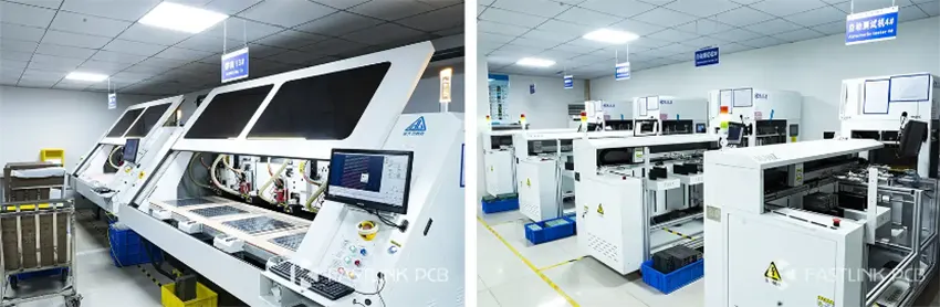
Our 65,000-square-foot state-of-the-art facility in Shenzhen houses the advanced equipment for manufacturing and assembling printed circuit boards. Fastlink leads the industry in quality and performance, whether you need standard fast PCBs or metal PCBs with tight tolerances.
There are more pictures of our factory’s equipment display in our company profile, please click here.
We are duly certified with the following accreditations:
● IATF 16949:2016
● ISO 9001:2015
● ISO14001:2015
● ISO13485:2016
● UL
Furthermore, all our products adhere to the IPC & ROHS Standards. It is our continuous endeavor to produce premium quality PCB products.