- [email protected] Mon-Sun 0. 00-23. 59
The PCB is an indispensable component within the electronics industry. The category of flexible PCBs encompasses a variety of types. Based on the structure of the flexible PCB, it can be classified into single-layer, double-sided, and multilayer variants, contingent on the number of conductor layers.
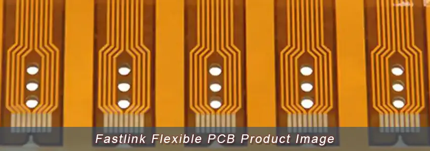
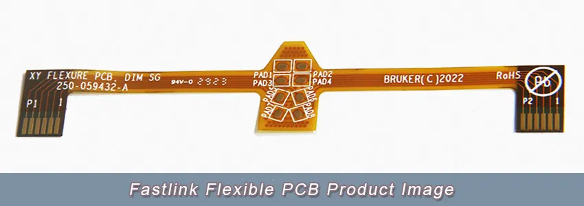
Fastlink provides a comprehensive array of PCB services, encompassing flexible, rigid-flex, and rigid PCB fabrication. This ensures that we are well-equipped to meet varied project requirements. We use premium-grade materials and the latest technology equipment to ensure our PCBs’ utmost performance and reliability.
The primary substrate of a flex PCB is typically made of polyimide (PI) or polyester. Polyimide, like Kapton, is popular because of its excellent thermal stability, chemical resistance, and flexibility. This base material provides mechanical flexibility to the PCB, allowing it to bend.
This layer, usually made of copper, is where the electrical connections are formed. Depending on the design and complexity, a flex PCB can have a single conductive layer or multiple layers. The copper can be either rolled or electro-deposited. The thickness of the copper layer varies depending on the current-carrying requirements.
It’s a protective layer applied over the conductive circuits. The coverlay provides insulation and protection against mechanical damage, contaminants, and moisture. It’s typically made of the same material as the base (like polyimide) but with an adhesive layer to stick it to the copper. Openings (windows) are made in the coverlay to expose pads for component soldering.
In areas where added rigidity is required, stiffeners are added. For instance, areas where connectors are attached or where components are mounted might need extra support. Common materials for stiffeners include polyimide, FR4, or metal.
These are used to bond the layers of the flex PCB together. The choice of adhesive often depends on the temperature requirements of the application. Thermoset adhesives are popular for high-temperature applications, while thermoplastic adhesives can be used for lower-temperature requirements.
If the flex PCB is multilayered, via holes might be used to interconnect layers. The vias can be plated with copper to ensure conductivity.
Depending on the design, flex PCBs might have specific termination areas like ZIF (Zero Insertion Force) contacts or might be designed to connect with rigid PCBs through connectors.
To ensure solderability and protection of the exposed copper pads, various surface finishes can be applied. Common surface finishes include Immersion Gold (ENIG), Immersion Tin, Immersion Silver, and OSP (Organic Solderability Preservative).
As their name suggests, Flex PCBs are inherently flexible. This allows for creative design solutions, accommodating intricate geometric configurations, bending, folding, or wrapping around curves without compromising the circuit’s integrity.
Flex PCBs can be significantly thinner than their rigid counterparts. This leads to considerable weight reduction, which is crucial in industries like aerospace and wearable technology. Additionally, their ability to be folded or bent means devices can be more compact.
Their ability to bend and flex can lead to less mechanical stress during regular use or vibrations, which in turn can result in a longer lifecycle. Moreover, the reduced number of interconnects can mean fewer solder joints and connectors, which are potential points of failure.
With fewer components, such as connectors, and the ability to integrate form and function, the assembly process can be simplified, reducing overall manufacturing costs.
The thinness of Flex PCBs allows for better heat dissipation in comparison to rigid PCBs. This can be crucial in high-performance applications where thermal performance is a concern.
Due to their flexibility, more components can be packed into a smaller space, leading to higher functionality per unit area.
Flex PCBs, especially when made from materials like polyimide, can withstand high temperatures and resist various chemicals. This makes them ideal for challenging applications like automotive or aerospace, where they might be exposed to fuels, solvents, or extreme temperatures.
Flex PCBs can be seamlessly integrated with rigid PCBs, leading to rigid-flex designs. This combines the best of both worlds – the versatility of flexible PCBs and the stability of rigid PCBs.
While the initial cost of Flex PCBs might be higher than rigid PCBs, the potential savings from reduced assembly costs, fewer components, improved reliability, and reduced need for replacement can make them more cost-effective in the long run.
Flexible materials might have dielectric constants that can benefit certain high-frequency applications. Additionally, the shorter interconnects can result in reduced signal loss and lower cross-talk.
Some applications require the continuous movement of the PCB (like in hinge areas of flip phones or in some medical devices). Flex PCBs are ideal for such applications due to their ability to move without failure repeatedly.
● Flexible PCBs, often called flex circuits, are crafted from materials like polyimide (PI) or polyester (PET), allowing them to bend and twist without harm. They’re ideal for tight spaces due to their thin and lightweight nature.
● Rigid-Flex PCBs merge the features of rigid and flexible circuits, integrating flexible circuitry with rigid sections, giving them a distinct design advantage.
● The primary attribute of flexible PCBs is their adaptability, permitting utilization in products requiring movement like wearables and medical instruments.
● Rigid-Flex PCBs, being both sturdy and adaptable, find their place in intricate electronic systems like aerospace apparatus and robotics.
● Flexible PCBs are notably resilient against mechanical stress and vibrations, making them apt for harsh environments.
● Rigid-Flex PCBs amplify this reliability by removing the need for connectors or solder joints between sections, ensuring better signal quality and reduced failure points.
● The specialized production process of flexible PCBs might elevate their cost over rigid PCBs, but the benefits they offer can counterbalance the initial expense.
● Rigid-Flex PCBs, though pricier than standard rigid PCBs, compensate with quicker assembly, better reliability, and notable space savings.
● Flexible PCBs are widely adopted in consumer electronics, aerospace, automotive, healthcare, and industrial sectors.
● Rigid-Flex PCBs are predominant in fields needing a blend of sturdiness and flexibility, such as defense systems, medical devices, and industrial machinery.
The primary material for Flex PCBs is typically polyimide (PI), known for its flexibility, heat resistance, and chemical stability. Another choice could be polyester (PET), though it’s generally used in less demanding applications due to its lower heat resistance.
Just like any PCB, the process begins with a circuit design. CAD (Computer-Aided Design) software is utilized to design the layout, which will later be used to produce a photographic film serving as a mask during etching.
The polyimide substrate is prepped and then coated with a copper layer on one or both sides, depending on the design. The copper can either be rolled on or electro-deposited.
Using the previously created photographic film, the circuit design is transferred onto the copper layer of the prepared substrate. This is usually achieved by applying a layer of photoresist, which is sensitive to ultraviolet light. The film is then placed over the substrate, and UV light is shone through. Where light penetrates, the photoresist hardens.
After imaging, the board is subjected to a chemical solution that etches away unprotected copper, leaving behind only the copper traces of the desired circuit design.
Post-etching, a protective layer, usually another layer of polyimide called a coverlay, is laminated onto the PCB to insulate and protect the copper traces. The coverlay has openings for component connections.
For multilayer flex PCBs, holes are drilled to make vias. These vias are then plated with copper to create connections between different layers. The plating is often accomplished through electroplating.
A thin layer of metal (often gold or tin-lead) is plated onto the pads to enhance solderability.
The individual PCBs are then cut or ‘profiled’ out from the larger production panel. This can be done using methods such as laser cutting, mechanical routing, or die cutting.
To further ensure solderability and protect the copper from oxidation, a surface finish is applied. Common finishes include Immersion Gold (ENIG), Immersion Tin, or OSP (Organic Solderability Preservative).
Components are then soldered onto the Flex PCB. Due to the sensitive nature of the material, care must be taken during assembly to prevent damage. Specialized equipment, like hot bar soldering machines, may be used to solder components.
Each Flex PCB undergoes electrical testing to ensure functionality and to check for shorts, opens, or incorrect connections.
It’s essential to note that the exact process can vary based on the manufacturer’s equipment, the design specifications, and the intended application of the Flex PCB. The manufacturing process requires precision and care, especially given the sensitive and flexible nature of the materials involved.
● Design for Manufacturability (DFM) Checks: Before production, design files undergo checks to ensure they meet manufacturing criteria.
● Stackup Selection: Determine the number of layers, material types, and thicknesses for the flex circuit.
● Layout Design: Place components, traces, vias, and other features on the board. Use specific design rules for flex PCBs like bending radii to prevent damage during use.
● Flex circuits primarily use polyimide films like Kapton as a substrate due to their flexibility, heat resistance, and electrical properties.
● Copper layers are adhered to these films, which will be etched to create the desired circuit pattern.
● Photo Imaging: Apply a photoresist material to the copper surface, expose it to UV light through a mask (representing the circuit pattern), and then develop to reveal the desired pattern.
● Etching: Remove the exposed unwanted copper using a chemical process.
● Stripping: Remove the remaining photoresist, leaving the desired copper circuitry.
Mechanical or laser methods are used to create holes for vias and component through-holes.
Electroplate the drilled holes to make them conductive, typically with copper, to connect different layers.
● Solder Paste Application: Apply solder paste to areas where components will be placed. This is usually done using a stencil.
● Component Pick and Place: Using specialized machines, components are picked from their tapes or trays and placed onto their corresponding positions on the flex PCB.
The board is passed through a reflow oven, where the solder paste melts, creating a solid bond between the component terminals and the PCB pads.
● Automated Optical Inspection (AOI): Machines scan the board for any defects like missing components, shorts, or solder bridges.
● X-Ray Inspection: Used especially for BGAs and other components that have hidden joints. This ensures there are no soldering defects underneath.
● In-Circuit Test (ICT): Checks for shorts, opens, resistance, capacitance, and other basic quantities.
● Functional Test (FCT): Tests the board’s functionality to ensure it operates as per design specifications.
● Cutting and Routing: The flex circuit is cut from the panel into individual units.
● Final Assembly: Depending on the application, this might involve attaching connectors, integrating into housings, or adding stiffeners for rigidity in certain areas.
● Coverlays: A protective film, usually polyimide, is added to protect the circuitry. This often has adhesive on one side to stick to the flex circuit.
● Surface Finishes: Techniques like ENIG (Electroless Nickel Immersion Gold) might be used to protect exposed copper pads from oxidation.
| Feature | Parameters |
| Material | PI, FPC, FCCL (35μm Cu + 25μm PI + 35μm Cu) Dupont |
| Structure | Flexible&Flex&Soft |
| Layer Count | 1-6 Layers |
| FPC Thickness | 0.002″ – 0.1″ (0.05-2.5mm) Including Stiffener Thickness |
| Coverlay | Single or Double Sided Yellow |
| Silkscreen | Single or Double Sided White |
| Surface Treatment | ENIGH or Immersion Gold |
| Finished Copper Weight | 1/3oz – 2oz |
| Min NC Drilling Dia | 0.2mm |
| Stiffener | PI, FR4, AL, 0.06mm steel stiffener |
| Minimum Trace/space | 3Mil/3Mill |
| Delivery Time | 1-2Weeks |
As a leading manufacturer from prototype to mass production of flexible PCBs, we have reliable technology in the manufacturing of flexible and rigid-flex PCBs. Our competitive edge lies in our ability to deliver boards with smaller line trace spaces and micro-vias. By partnering with us as your flexible circuit supplier, you will have access to our high-quality flex PCB design and engineering services. Our experienced team will assist you in identifying the most suitable technologies for your project’s specific application.
We are duly certified with the following accreditations:
● IATF 16949:2016
● ISO 9001:2015
● ISO14001:2015
● ISO13485:2016
● UL
Furthermore, all our products adhere to the IPC & ROHS Standards. It is our continuous endeavor to produce premium quality PCB products.