- [email protected] Mon-Sun 0. 00-23. 59
Helping our customers bring new products to market in a fast, efficient and highly strategic manner is what makes us stand out as an electronic contract manufacturer like Fastlink Electronics.
In the early stages of new design work, Fastlink Electronics strives to mitigate future production barriers and aims to optimize the production capacity of the product while keeping overhead costs low. Based on our actual manufacturing experience in past projects.
Design PCB products especially suitable for PCB assembly equipment and batch manufacturing process for customers.
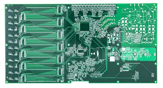
Printed Circuit Board (PCB) layout is the process of arranging and connecting electronic components on a printed circuit board to form a functional electronic circuit. The layout is a critical part of the design process as it determines the performance, reliability, and manufacturability of the final product.
Design for Manufacturability (DFM) principles are guidelines that ensure that the PCB design is optimized for efficient and cost-effective manufacturing. The DFM guidelines consider factors such as the type of components used, the size and shape of the PCB, the placement of components, and the routing of traces. By following DFM principles, designers can reduce manufacturing costs, improve product quality, and decrease time-to-market.
Design for Manufacturability (DFM) is a set of principles that help ensure that a PCB design is optimized for efficient and cost-effective manufacturing. Some of the key DFM principles include:
Selecting components that are readily available, standard, and easy to mount on the PCB can reduce manufacturing costs and lead times.
Choosing the right size and shape of the PCB can help optimize panel utilization during PCB fabrication, reducing waste and lowering manufacturing costs.
Proper placement of components can help reduce the length of traces, which in turn can improve signal integrity, reduce noise, and improve reliability.
Careful routing of traces can help avoid signal interference, reduce crosstalk, and improve signal integrity. Using the shortest path between two points can help reduce the length of traces and improve signal quality.
Adhering to design rules for trace width, spacing, and clearance can help ensure that the PCB is manufacturable and meets the requirements of the PCB fabrication process.
Grouping multiple PCB designs onto a single panel can help optimize the use of manufacturing resources, reduce costs, and improve production efficiency.
Designing the PCB for ease of testing can help reduce the time and cost of testing during manufacturing, and improve the quality and reliability of the final product.
By following these DFM principles, designers can improve the manufacturability of their PCB designs, reduce manufacturing costs, and improve product quality and reliability.
PCB layout guidelines are a set of principles that help ensure that a PCB design is optimized for performance, reliability, and manufacturability. A well-designed PCB layout can help reduce noise, ensure signal integrity, and improve overall system performance. Some of the key PCB layout guidelines include:
Component placement
Proper placement of components can help reduce the length of traces, which in turn can improve signal integrity, reduce noise, and improve reliability. Critical components should be placed first and should be located as close as possible to their associated connectors and power supplies.
Trace routing
Careful routing of traces can help avoid signal interference, reduce crosstalk, and improve signal integrity. High-speed traces should be routed as short and direct as possible, and should be separated from each other to minimize crosstalk.
Power and ground planes
Proper placement of power and ground planes can help reduce noise, improve signal integrity, and provide a stable reference for the circuit. Power and ground planes should be placed close to each other and should be connected through multiple vias to reduce impedance.
Signal integrity considerations
High-speed signals should be routed with impedance-controlled traces to maintain signal integrity. Differential pair routing should be used for high-speed differential signals, and length matching should be performed to ensure that signals arrive at their destination at the same time.
Design rule check (DRC)
DRC is a software tool that checks the PCB layout against a set of design rules to identify potential manufacturing issues. DRC rules include trace width, spacing, and clearance, and can help ensure that the PCB is manufacturable and meets the requirements of the PCB fabrication process.
By following these PCB layout guidelines, designers can ensure that their PCB designs are optimized for performance, reliability, and manufacturability.
Because so many industries use PCBs, they are almost everywhere, from small consumer equipment to large mechanical equipment. Fastlink Electronics has helped our customers from different industries with design work of pcb assembly and manufacturing:
Here are some best practices for PCB layout and DFM:
Plan ahead: Before starting the PCB layout, it’s important to have a clear understanding of the design requirements and constraints. This includes the type of components used, the size and shape of the PCB, and the expected performance characteristics.
Use a schematic capture tool: A schematic capture tool can help ensure that the PCB layout is accurate and consistent with the design requirements. The schematic capture tool can also help automate some of the design processes, such as generating netlists and component footprints.
Follow DFM guidelines: Following DFM guidelines can help ensure that the PCB design is optimized for efficient and cost-effective manufacturing. This includes selecting components that are readily available, standard, and easy to mount on the PCB, as well as optimizing the size and shape of the PCB to reduce waste and lower manufacturing costs.
Use a PCB layout tool:A PCB layout tool can help automate the layout process and ensure that the design meets the requirements of the PCB fabrication process. The layout tool can also help with trace routing, component placement, and other design tasks.
Perform design rule checks: Before finalizing the PCB layout, it’s important to perform design rule checks (DRC) to identify potential manufacturing issues. The DRC tool checks the design against a set of rules to ensure that the design is manufacturable and meets the requirements of the PCB fabrication process.
Use high-quality components: Using high-quality components can help improve the reliability and performance of the final product. This includes selecting components that meet the required specifications and have a proven track record of reliability.
Test the design: Testing the design before finalizing the layout can help identify potential issues and ensure that the design meets the required performance characteristics. This includes performing simulations, testing prototypes, and verifying the design against the design requirements.
PCB layout and DFM are critical aspects of the electronic design process. A well-designed PCB layout can help improve the performance and reliability of the final product, while DFM principles can help reduce manufacturing costs and improve time-to-market. By following best practices for PCB layout and DFM, designers can optimize their designs for performance, reliability, and manufacturability.