- [email protected] Mon-Sun 0. 00-23. 59
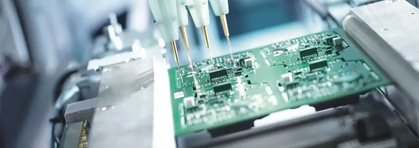
Through-hole assembly is a technique in electronics where connections are established by inserting components through holes in a circuit board. This method has been a prevalent choice for producing Printed Circuit Board Assemblies (PCBAs) for many years. Despite the advent of newer assembly methods, through-hole PCB assembly remains in demand due to its simplicity, reliability, and cost-effectiveness. It’s commonly used for prototype development and small-scale production. At Fastlink, our through-hole manufacturing services encompass a broad range of capabilities, including automatic component insertion, wave soldering, and selective soldering processes. Additionally, we provide automated insertion of both radial and axial components.
In the last three decades, the electronics industry has increasingly favored surface-mount technology (SMT). This trend is largely driven by cost factors. SMT components are not only more compact but also typically less costly. However, despite their economic benefits, SMT solder joints are prone to various manufacturing defects like cracking, voids, and solder balls, making them less reliable in certain scenarios. Consequently, through-hole technology maintains its relevance in specific applications.
For large-scale production, automated through-hole PCB assembly is feasible using equipment for axial, radial, or Dual In-line Package (DIP) insertion. Once components are positioned in the designated through holes, the soldering process follows. This can be done manually or through additional automation. For bulk production involving repetitive through-hole soldering, processes like automated wave soldering or selective soldering are commonly employed.
Fastlink employs both manual and automated through-hole assembly techniques for radial and axial components. For small-volume production, automated through-hole PCB assembly is our preferred method, reducing material handling and labor costs. Our manual technique tackles complex through-hole assembly challenges, minimizing operator movement and product travel. Documentation and in-process checks ensure complete and accurate component placement.
Wave soldering is used for both through-hole and surface mount components, but we favor it for through-hole components. Mixed technology PCBs undergo both reflow and wave soldering processes.
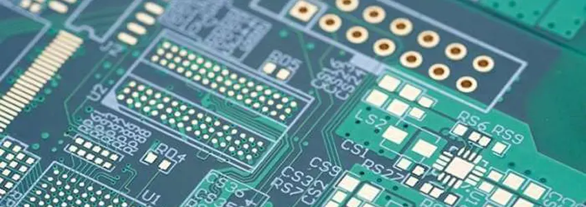
● Through-hole PCB assembly involves connecting components through pre-drilled holes on the circuit board, with soldering done on both sides for secure attachment.
● This technology is well-suited for crafting complex, large-scale circuits, particularly in high-frequency applications.
● Due to their larger size and robust connection points, through-hole components are capable of managing higher current loads compared to their surface mount counterparts.
● Through-hole PCBs can accommodate heavier components like connectors, potentiometers, and switches, which often aren’t suitable for SMT assemblies.
● These boards excel in heat dissipation, offering a larger contact area between the component and the circuit board through metal plating or solder, which is a significant advantage over SMT.
● In terms of electrical performance, through-hole technology surpasses others like SMD/SMT, offering enhanced signal integrity, EMI shielding, and ground plane designs.
● Repair and rework are more straightforward with through-hole boards as they provide easy access to both sides of the circuit board, unlike surface mount technology.
● Through-hole technology is recognized for its higher reliability due to its strong mechanical connections, making it a preferred choice for applications where a stable connection is critical.
● The larger size and more robust electrical connections of through-hole boards make them more tolerant to temperature variations, shocks, and vibrations compared to SMT, ideal for demanding environments.
In the realm of circuit assembly, surface mounting is widely adopted across various industries. Nonetheless, PCB through-hole assembly remains indispensable for circuits in equipment that must withstand high stress, operate at elevated speeds, or endure extreme temperatures. Through-hole PCB assembly is chosen for these applications due to its several advantages:
Through-hole assembly involves inserting components into a circuit board and securing them with metal solder. This method creates robust connections between the circuit and its components, essential for maintaining the integrity of electrical equipment during use. This strength makes through-hole assembly a preferred choice for high-risk electrical equipment over other methods like surface mounting.
The stronger bonds between the circuit and its components mean enhanced durability. This quality allows the assembly to withstand harsh conditions with minimal wear or damage. Through-hole assembly is particularly suitable for sectors like aerospace or heavy machinery, offering greater longevity and potentially reducing the need for frequent replacements.
Reliability is a key concern when using machinery, and through-hole PCB assembly addresses this issue effectively. The reliability of drilling and soldering technology in through-hole assembly eliminates uncertainties regarding the performance of the circuit. This reliability is crucial in maintaining efficiency, especially in demanding or fast-paced operational environments.
Through-hole assembly is recognized for its eco-friendliness and the robust connections it forms between components and the board. This method moves away from traditional soldering approaches, reducing environmental stress. Its high reliability makes it particularly suitable for industries with stringent requirements, such as aerospace and military. The through-hole process involves inserting component leads into the PCB holes and soldering them, creating a bond capable of withstanding mechanical stress and high temperatures, a key reason for its prevalence in military and aerospace equipment manufacturing.
In the realm of PCB production, through-hole components are a staple, especially for testing and prototyping phases. Their design allows for easier replacement and repositioning compared to standard components, enhancing the versatility and convenience in various applications. The durability and stress tolerance of through-hole components also make them a popular choice in industrial equipment and machinery. In addition, the robust and bright features of through-hole LED lights have made them a favored option for large-scale displays like giant billboards.
Despite its advantages, through-hole assembly has its limitations. The process can be both time-consuming and costly, primarily due to the drilling required and the necessity of manually inserting and soldering the components. This labor-intensive method can extend production timelines and increase costs, factors important to consider in high-volume manufacturing environments.
Another limitation of through-hole assembly lies in its suitability for multi-layer PCBs. The requirement for drilling holes through multiple layers can complicate the design and reduce the efficiency of the board. Additionally, through-hole PCBs tend to be larger than their surface mount technology (SMT) counterparts. This size difference can limit their application in contexts where compactness and space efficiency are crucial.
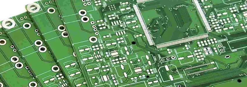
At Fastlink, we offer through-hole PCB assembly services that cater to the conventional lead assembly needs across diverse industries. Our services encompass single, double-sided, and high-density multilayer Plated Through Hole (PTH) circuit board assembly, aligning with the low to mid-volume production demands of our clients. Our developed capabilities over the years enable us to serve our clients more effectively:
● We specialize in PCB through-hole assembly for single, double-sided, and high-density multilayer boards.
● Our facility is equipped with advanced automated insertion equipment for axial and radial components, facilitating rapid and precise installation of through-hole components.
● We utilize state-of-the-art reflow ovens for optimal solder paste application, along with automated wave soldering equipment to ensure accurate soldering of through-hole components.
● Our comprehensive testing capabilities, including in-circuit testing, automated optical inspection (AOI), automated X-ray inspection (AXI), and burn-in tests, ensure we maintain both quality and affordability.
● Fastlink has a track record of successfully handling low to high volume projects for clients in sectors like aerospace, medical, automotive, and telecommunications.
A critical aspect of our PCB manufacturing and assembly is rigorous product testing. Upholding quality standards is a cornerstone of our operations, reflected in our meticulous testing and inspection processes.
Delivering electrical components without thorough inspection increases the risk of malfunctions, which can disrupt business operations. Our advanced automated testing and inspection systems identify defects early, ensuring the reliability of our PCBs before they reach our clients.
Our capabilities extend to handling a variety of projects, regardless of the PCB design or size. We work efficiently with both standard and custom materials, including copper, rigid FR-4, flex, Rogers, rigid-flex, and aluminum. Our procurement process is flexible, sourcing components necessary for PCB assembly and accommodating materials provided by clients. This approach allows us to offer unique and cost-effective assembly solutions tailored to each project’s specific needs.