- [email protected] Mon-Sun 0. 00-23. 59
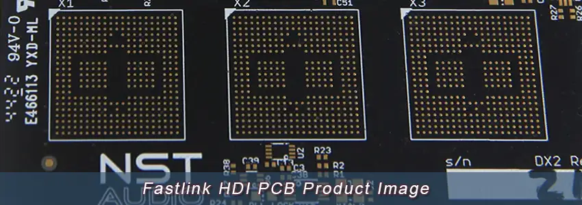
High-density interconnect (HDI) PCBs are circuit boards with a higher number of interconnections per square inch than traditional PCBs. This results in smaller, more compact circuit boards. HDI PCBs can be used to reduce the size of electronic devices, such as smartphones and laptops, without sacrificing functionality.
HDI PCBs incorporate dense component placement and versatile routing. They also use microvias, buried vias, and blind vias to create denser circuitry. Microvias are smaller than traditional vias, which allows for more routing options and reduces the drill-to-copper ratio.
Fastlink’s PCB manufacturing provides high-quality HDI PCBs at competitive prices, without a minimum order quantity requirement. Our team performs design for manufacturability checks on your custom PCB file and consults with you to ensure that it is ready for manufacturing and meets your performance requirements.
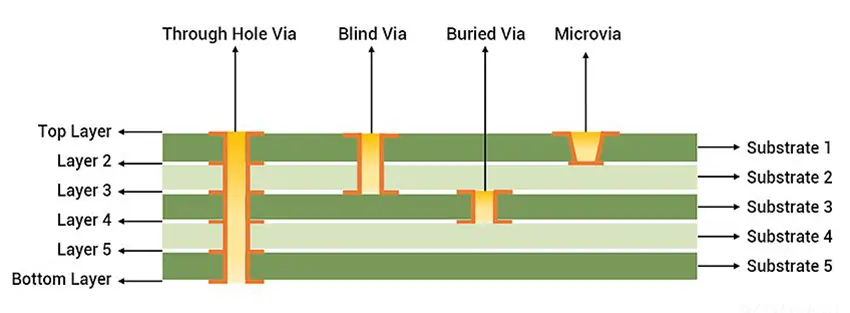
A via is a small conductive hole that connects multiple layers of an HDI PCB, allowing signals to pass between them. There are four types of vias used in HDI PCBs:
● Through-hole vias: These vias extend from the top to the bottom layer of the PCB.
● Blind vias: These vias connect an inner layer to a surface layer of the PCB.
● Buried vias: These vias connect two inner layers of the PCB.
● Microvias: These vias are smaller than through-hole vias and are often used in HDI PCBs to connect multiple layers without increasing the size of the board.
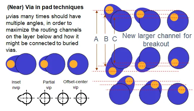
HDI PCBs require vias that are typically at the lower limit of what can be mechanically drilled. For vias smaller than 6 mils, an alternative formation process is needed to place microvias between layers. Filled plated microvias are a standard feature on HDI PCBs and can be used in a via-in-pad design approach to increase density. Via-in-pad is a simple way to pack more components into a design, as it provides a direct connection from a component lead to an internal layer.
When there are reliability concerns regarding microvias, a near-pad technique can be used. In this approach, a very small trace section comes off from a pad and touches the microvia. This completes the connection to an internal layer and provides a larger breakout channel if drill wander causes the microvia to be drilled slightly off center.
Embracing HDI technology, designers gain the versatility to populate both sides of the raw PCB with more components. Various via methodologies, such as via in pad and blind via technology, furnish designers with additional PCB real estate, enabling the placement of smaller components in closer proximity. The reduction in component size and pitch facilitates an increase in I/O within smaller geometries. Consequently, this yields quicker signal transmission along with a noteworthy reduction in signal loss and crossing delays.
The choice of material and its construction is pivotal in the design and manufacturing of HDI (High-Density Interconnect) PCBs. The process of designing HDI interconnects entails a comprehension of potential challenges associated with specifying glass reinforced dielectric materials.
Microvia dielectric materials might engender misregistration and rough vias, irrespective of the drilling technique employed—be it plasma, laser, or mechanical. The concerns extend beyond the inherent material properties of the microvia dielectric materials to the consistency of the weave and the caliber of fibers used. The ability to narrow the weave openings by spreading the fibers is crucial, as it diminishes open spaces that can lead to skew and drift.
● Copper Clad Laminate (CCL): Copper clad laminate materials involve the lamination of copper foil to one or both sides of a cured (C-stage) dielectric. The rigid CCLs may be categorized as FR4, FR-5, or certain PTFE types. A typical application employs single-side clad laminate material, where the copper clad serves as the outer layer, and the C-stage is bonded to the sub-composite. Microvias are created using laser drilling techniques. The materials vary based on reinforcement (woven glass, non-woven glass, and expanded PTFE) and the chemistries at play (epoxies, polyimide, polyester, etc.).
● Resin Coated Copper (RCC): Resin coated copper materials consist of copper foil coated with a resin dielectric material, which can be directly bonded to the sub-composite. They are distinguished by their processability in a wet environment or lack thereof. For non-wet processable-coated copper materials, microvias are created using either plasma or laser drilling techniques.
● PP (Prepreg): Often referred to as B-stage, Bonding sheet, or simply Preg, Prepreg comprises fiberglass fabric impregnated with resin. During the Prepreg coating operation, the resin undergoes partial curing without hardening. During the heating phase of the PCB stack-up in the pressing process, the resin in PP will flow, adhere, and bond the PCB core with copper foil or other materials.
● Sequential Lamination: During lamination, PCB core or cores are fused with copper and, in the case of multi-layer PCBs, with pre-preg layers, utilizing heat and pressure. The requisite heat and pressure fluctuate across different boards. Post-lamination, the manufacturer drills vias into the PCB. Unique to HDI boards is the repetition of this process, which aids in averting misalignments and fractures during drilling.
● Via-in-Pad Process: This procedure enables the placement of vias on the PCB’s flat lands by plating the via, filling it with a selected material, capping, and then plating over it. Typically comprising 10 to 12 steps, this process mandates specialized equipment and adept technicians. It’s a prudent choice for HDI PCBs, facilitating improved thermal management, space conservation, and offering an efficient route to bypass capacitors in high-frequency designs.
● Via Fill Types: The selection of via fill should align with your application and PCB specifications. Commonly used fill materials include electrochemical plating, silver-filled, copper-filled, conductive epoxy, and non-conductive epoxy, with the latter being prevalent. Ideal fills meld seamlessly with the flat land, akin to traditional lands, and accommodate both microvias and standard vias to be blind, buried, or drilled, then plated to obscure them beneath SMT lands. Precise control over drill cycles at defined depths is essential, requiring specialized equipment and an extended development timeframe.
● HDI Structures: HDI PCBs offer a variety of layout choices like 1-n-1 PCB and 2-n-2 PCB. The 1-n-1 PCB embodies a singular high-density interconnect layer build-up, mandating one sequential lamination on each core side. Conversely, the 2-n-2 PCB hosts two HDI layers, allowing for staggered or stacked microvias across layers. Complex designs may feature copper-filled stacked microvia structures, although the ascent to higher X-n-X levels is often curtailed by cost and complexity. The any-layer HDI, a denser layout enabling free interconnection among conductors on any layer with laser microvia structures, is notable, especially in smartphone GPU and CPU chips.
● Laser Drill Technology: Any-layer HDI designs frequently necessitate laser microvias, created using laser drills capable of generating up to 20-micron diameter lasers to precision-cut both metal and glass, yielding minuscule yet pristine holes. Utilizing materials like uniform glass with a low dielectric constant can further shrink hole dimensions.
● LDI and Contact Imagery: As a leading HDI PCB supplier, Fastlink pushes the envelope with cutting-edge technology and clean rooms to deliver finer lines with safe and secure processing. For these delicate details, repairs are impossible, so it is essential to do it right with extreme precision the first time. We alternate between contact imaging and LDI imaging based on your equipment verification needs. LDI is the go-to for fine lines and minute spacing, as it can verify even the most demanding processes. This continually expands our capabilities and allows for smaller form factors.
The design of an HDI PCB is critical to its successful manufacturing. HDI PCB design must carefully consider the following factors:
● Line width and spacing: HDI PCBs typically have line widths and spacings of 1 mil or less. This requires precise design and manufacturing techniques to ensure that the traces are properly formed and that there is no electrical interference between traces.
● Via size and placement: HDI PCBs often use microvias, which are vias with a diameter of 6 mils or less. Microvias are more difficult to drill and plate than traditional vias, so they must be carefully placed on the PCB.
● Stack-up: HDI PCBs often have complex stack-ups, with multiple layers of copper and dielectric material. The stack-up must be carefully designed to ensure that the PCB is electrically and mechanically sound.
Photolithography is a process used to transfer the PCB design from a CAD file to a copper-clad laminate (CCL) board. The process involves the following steps:
1. A photosensitive coating is applied to the CCL board.
2. The PCB design mask is placed over the photosensitive coating.
3. The board is exposed to ultraviolet light.
4. The photosensitive coating is developed, removing the coating from the areas that were not exposed to light.
5. The copper is etched from the areas where the photosensitive coating was removed.
Etching is a process used to remove the unwanted copper from the CCL board. The board is immersed in an acidic solution that dissolves the copper that is not protected by the photosensitive coating.
Drilling is used to create the vias in the PCB. Vias are small holes that connect the different layers of copper on the PCB. HDI PCBs often use microvias, which are vias with a diameter of 6 mils or less. Microvias are more difficult to drill than traditional vias, so specialized equipment is required.
Plating is used to deposit copper onto the vias and traces on the PCB. This is done by immersing the board in an electroplating solution. The electroplating solution contains copper ions, which are deposited onto the board by an electric current.
Lamination is a process used to apply a protective layer of solder mask to the PCB. The solder mask is a green or blue coating that protects the copper from oxidation and prevents solder from bridging between traces.
Once the PCB has been laminated, it is tested to ensure that it meets all of the specifications. This is done using a variety of electrical and optical tests.
The final step in the HDI PCB manufacturing process is to apply a finish to the board. The finish can be either a conformal coating or a hot air leveling (HAL) finish. A conformal coating is a thin layer of material that is applied to the board to protect it from moisture and corrosion. A HAL finish is a thin layer of solder that is applied to the board to protect the copper from oxidation and to improve solderability.
In addition to the basic steps listed above, there are a number of extensions that can be used to enhance the functionality and performance of HDI PCBs. Some of these extensions include:
● Sequential lamination: Sequential lamination is a process used to create PCBs with multiple layers of copper and dielectric material. This process allows for the creation of complex stack-ups that are not possible with traditional PCB manufacturing methods.
● Laser direct imaging (LDI): LDI is a process used to transfer the PCB design to the CCL board using a laser. LDI is more precise than traditional photolithography methods, and it can be used to create PCBs with finer line widths and spacings.
● Plasma-enhanced chemical vapor deposition (PECVD): PECVD is a process used to deposit a thin layer of dielectric material onto the PCB. This process can be used to create vias and traces with smaller dimensions and tighter tolerances.
High-Density Interconnect (HDI) PCBs are integral to a plethora of sophisticated electronic devices demanding high performance alongside space efficiency. These PCBs find ubiquitous applications across mobile phones, touchscreen gadgets, laptops, digital cameras, and next-gen network communications like 4G/5G, not to mention critical military applications such as avionics and smart munitions. The compactness and enhanced performance of HDI PCBs address the requisite intricacies and space constraints inherent in these domains, thereby significantly contributing to their operational efficacy.
In the automotive and aerospace sectors, the adoption of HDI PCBs is on an upswing, driven by the imperative of reducing weight to boost operational efficiency. Modern automobiles are morphing into highly connected, computerized entities, hosting around 50 microprocessors that oversee a gamut of functionalities ranging from engine control, diagnostics, and safety protocols to myriad conveniences. Key advanced features like onboard Wi-Fi, GPS, rearview cameras, and backup sensors are underpinned by HDI PCBs. As automotive technology gallops ahead, the role of HDI technology is poised to burgeon, underpinning the evolution of smarter, more efficient vehicles.
The medical and industrial automation spheres are other prominent arenas where HDI PCBs make a substantial impact. Advanced medical devices crucial for monitoring, imaging, and surgical endeavors heavily rely on HDI boards to achieve enhanced performance and cost-effectiveness, potentially augmenting the precision of medical monitoring and testing procedures. On the industrial front, as automation and IoT devices permeate manufacturing and warehousing operations, HDI technology becomes indispensable. The modern industrial milieu leverages electronic tools for inventory management and equipment monitoring, with machinery increasingly outfitted with smart sensors. These sensors, facilitated by HDI technology, collate usage data, interface with the internet to interact with other smart devices, and relay pivotal information to management, thereby aiding in optimizing operational paradigms.
| Specifications | PCB Capabilities |
| PCB Layers | 4 ~34 layers |
| High-Density Layers | Up to 18 layers |
| Delivery Time | 1 day to 3 weeks |
| Stackup | 1+N+1, 2+N+2, 3+N+3, 4+N+4 |
| PCB Via | Blind via, Buried via, Staggered via, Stacked via, Skip via |
| Minimum Laser Drill Diameter | 0.075mm |
| Final PCB Thickness | 0.15mm |
| Minimum Trace Width/Space | Flex/rigid-flex PCBs: 1.6mil/1.6mil Rigid PCBs: 3mil/3mil |
| Production Capability | 3000m² per day |
| Copper Thickness | 100μm to 125μm |
| Impedance Control | 90Ω ~100Ω |
| Technical Feature | 90Ω & 100Ω Differential impedance, thick cooper |
| Silkscreen | White, Black, Red,etc. |
| Soldermask | Green, Blue, Purple, White, Black, Pink,Orange |
| Surface finish | OSP, HASL, Lead Free HASL,ENIG,Immersion Tin,Immersion silver, Hard gold plating,etc. |
Fastlink is a Shenzhen-based HDI PCB manufacturer and provider that offers prototyping and mass production at competitive prices and with quick turnaround times. We serve a wide range of industries, and our customers all have high expectations for quality, reliability, and on-time delivery. Quality is not an afterthought for us; it is built into every step of the process, from front-end design to fabrication to shipping.
Fastlink’s equipment gives our customers the power to maximize the functionality and performance of their HDI PCB designs in less space by using microvias, blind vias, via-in-pad, stacked vias, and staggered vias. We achieve high precision with laser drilling capabilities, such as precise depth control. Our Laser Direct Imaging (LDI) capabilities ensure exact registration and proper inspection of all inner layers.
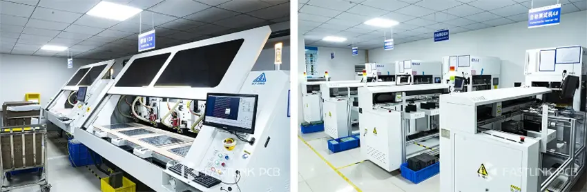
Our 65,000-square-foot state-of-the-art facility in Shenzhen houses the advanced equipment for manufacturing and assembling printed circuit boards. Fastlink leads the industry in quality and performance, whether you need standard fast PCBs or metal PCBs with tight tolerances.
There are more pictures of our factory’s equipment display in our company profile, please click here.
We are duly certified with the following accreditations:
● IATF 16949:2016
● ISO 9001:2015
● ISO14001:2015
● ISO13485:2016
● UL
Furthermore, all our products adhere to the IPC & ROHS Standards. It is our continuous endeavor to produce premium quality PCB products.