- [email protected] Mon-Sun 0. 00-23. 59
Whether rigid or flexible, high-frequency PCBs enable faster signal transmission rates and support operating frequencies up to 100 GHz. Their performance is enhanced by materials specifically selected for their low dielectric constant (Dk), low dissipation factor (Df), and minimal thermal expansion. HF PCBs are commonly used in high-density interconnect (HDI) technology and are essential components in high-speed communications, telecommunications, and radio frequency (RF) microwave applications.
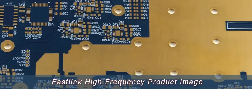
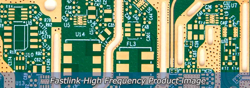
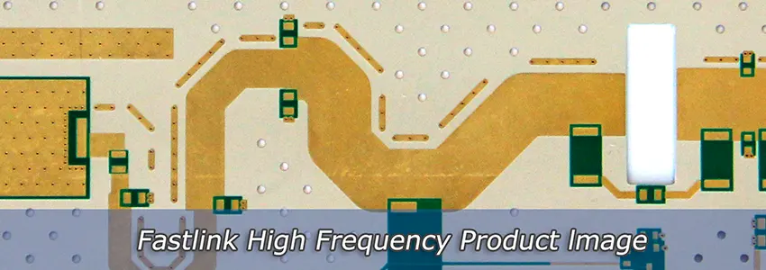
Fastlink is a China-based professional PCB manufacturer that offers reliable and high-performance high-frequency PCB fabrication services. We can produce high-frequency PCBs typically in the range of 500MHz to 10GHz.
1. Dissipation Factor (Df): High-frequency PCBs have a low dissipation factor, which typically falls between 0.0019 and 0.025. This low Df is crucial for maintaining the signal transmission rate, minimizing signal loss, and enhancing signal transmission.
2. Dielectric Constant (Dk): The dielectric constant in HF PCBs is lower and stable, which is vital for ensuring efficient frequency transmission and reducing signal delay. A lower Dk helps in improving frequency transmission capabilities.
3. Chemical Resistance: These PCBs can tolerate exposure to chemicals, which means they are less likely to corrode or suffer damage in environments where chemical exposure is a risk.
4. Moisture Absorption: HF PCBs are designed with materials that have a low rate of water absorption, allowing them to perform reliably in humid environments without degradation of their electrical properties.
5. Dimensional Stability: They exhibit low dimensional stability, meaning that they maintain their shape and size irrespective of the temperature they are exposed to, whether it is heat or cold climates.
6. Thermal Conductivity: Most high-frequency PCB substrates have low thermal conductivity, in the range of 0.2–0.3 W/m/K. To manage heat effectively, a thinner substrate may be used to shorten the heat flow path to the heat sink. However, a thinner substrate can lead to more heat generation due to RF heating. Conversely, a thicker substrate with lower insertion loss can generate less RF heat but has a longer heat flow path, which can be mitigated if the substrate has a very low dissipation factor.
7. Material Choices: The materials used in HF PCBs, like Teflon and newer generation substrates, are chosen for their low Dk and Df, water absorption properties, and survival in various environments. Materials such as FR4 are less expensive but may not perform well at signal speeds above 1.6 GHz, whereas Teflon and flex substrates are better for high-frequency applications above 10 GHz.
8. Thermal Management Materials: Some laminates claim high thermal conductivity and low loss. RT/Duroid 6035HTC, for instance, has a very low dissipation factor and extremely high thermal conductivity at 1.44 W/m/K. Selecting the right material is crucial for high-frequency, high-power PCB applications to ensure proper thermal management.
1. Materials: HF PCBs are made from specialized materials with low dielectric constant (Dk) and low dissipation factor (Df). Dk measures how much a material slows down an electrical signal, while Df measures how much energy is lost as heat. Low Dk and Df minimize signal distortion and attenuation at high frequencies.
2. Trace Geometry: The geometry of the traces, the conductive paths on the PCB, is crucial for high-frequency performance. Trace widths and spacing must be carefully controlled to minimize signal reflections and crosstalk, which can interfere with signal integrity.
3. Grounding and Power Distribution: Proper grounding and power distribution are essential for HF PCBs to ensure stable signal transmission and minimize noise. Ground planes, dedicated power planes, and decoupling capacitors are commonly employed to achieve this.
4. Fabrication Techniques: HF PCBs require specialized fabrication techniques to ensure precise alignment of traces, vias, and other components. Laser direct imaging (LDI) and controlled impedance drilling (CID) are often used to achieve the required accuracy.
High-frequency PCBs work by using specialized materials and design techniques to handle signals that operate at high frequencies, which are typically above 1 GHz. These signals require smooth copper surfaces, low dielectric constant materials, and tight control of impedance to minimize signal losses and distortion. The PCB’s substrate is often made from materials like PTFE (Teflon) or advanced resin to maintain signal integrity. The design may include microstrip or stripline configurations to manage the path of the signals, and the layout is optimized to prevent crosstalk and electromagnetic interference, which are critical at high frequencies.
The Rogers RO4000 series has been an industry leader. As a low-loss material, it’s frequently used in microwave and millimeter-wave frequency designs. Its ease of use in circuit production and consistent performance offer advantages over conventional PTFE materials.
Specifically, Rogers 4350B exhibits low loss and is suitable for applications in the 500MHz to 3GHz frequency range. Panasonic Megtron 6 is another low-loss material that is designed for the higher frequency range of 3GHz and above. Materials such as Isola I-speed, Isola Astra, and Tachyon exhibit excellent low-loss characteristics at high frequencies.
1. Minimize Noise: Design strategies must aim to reduce electromagnetic interference (EMI), a significant disruption source in high-frequency PCBs.
2. Understand Frequency and Speed: High-frequency PCBs are concerned with the rate of signal change, which affects signal integrity due to impedance and other board parameters1.
3. Material Selection: Use materials with stable dielectric constants at high frequencies and choose copper with a smooth, low-profile surface to minimize losses.
4. Component Placement: Components should be grouped by signal type, with special attention to isolate high-radiation components like antennas.
5. Trace and Space Management: Maintain consistent spacing between differential traces and adhere to creepage and clearance standards.
6. Routing Considerations: Route different signal types on separate layers, minimize trace lengths, and maximize spacing between traces to prevent interference.
7. Stackup Configuration: Employ a symmetric stackup when possible, which helps maintain consistent impedance across the PCB.
8. Grounding Techniques: Use separate grounds for different signal types and avoid splitting ground planes, as this can introduce noise.
9. Filtering and Shielding: Implement proper filtering for fast-switching signals and apply shielding to components that radiate high levels of EMI.
The fabrication of a high-frequency PCB begins with finalizing the board stack-up, which is the arrangement of various layers to ensure optimal performance. This critical step determines the dielectric properties and signal integrity. Once the stack-up is confirmed, layout design commences, routing signal tracks via specialized software, creating a blueprint that guides the subsequent fabrication steps.
Digital designs are transformed into physical films using a plotter printer, which prints the conductive and non-conductive areas with different inks. This stage is vital for accuracy in the etching process, as it delineates where copper should be preserved or removed.
The inner copper layers are prepared by first cleaning the copper-clad laminates to eliminate contaminants. These laminates, coated with photoresist, are then exposed to UV light, which hardens the photoresist in the areas that will become the circuit traces, ensuring precision in the pattern that will form the electrical pathways.
The etching process selectively removes unwanted copper, leaving behind the circuit pattern. This is achieved by washing away unhardened photoresist and then etching the exposed copper with an alkaline solution. This step requires precise control to maintain the integrity of the desired circuitry.
Each layer undergoes Automated Optical Inspection (AOI) against the design files to detect and correct any errors. Precise drilling of registration holes aligns the multiple layers in preparation for lamination, highlighting the importance of dimensional accuracy.
The layers are bound together using heat and pressure to melt prepreg material, forming a solid board structure. The drilling of vias and holes follows, incorporating X-ray alignment for accuracy, which is particularly crucial for maintaining the conductive paths in high-frequency applications.
The outer layers undergo similar preparation as the inner layers. Electroplating follows, depositing a conductive material on the walls of the drilled holes and vias to establish a continuous electrical pathway critical for signal transmission.
A solder mask is applied to protect the copper traces and prevent electrical shorts. Silkscreen printing then adds labels and component information, providing a guide for assembly and usage.
The final step is a comprehensive testing phase that ensures the PCB’s functionality by checking for continuity and proper isolation. After successful testing, the PCB is cut into individual boards, ready for delivery to the customer.
High-frequency PCBs are commonly used in applications where high-speed signal transmission is required, such as telecommunications, radar, and defense systems. Because of their unique properties, they are able to maintain signal integrity and minimize signal loss, which is crucial for these applications.
● In cellular networks, satellite comms, and wireless tech, HF PCBs facilitate signal transmission.
● Radar systems utilize them to emit and capture radio waves for object detection and tracking, aiding in air traffic, weather prediction, and security.
● Within defense, they’re integral to electronic warfare and communication devices, enduring extreme conditions.
● Medical imaging devices like MRI and X-ray machines rely on them for high-definition data transfer.
● Scientific tools, including oscilloscopes and spectrum analyzers, depend on them for precise high-frequency signal analysis.
● Automotive uses include radar for safety features and adaptive cruise control.
● In aerospace, they’re critical for communication and radar, designed to perform in demanding environments.
In addition to these applications, HF PCBs are also used in a variety of other industries, including consumer electronics, industrial automation, and transportation.
| Feature | Capability |
| Layer Counts | 1-36 |
| Normal Lead Time | 4-6 Working Days |
| Fast Lead Time | 1-2 Working Days |
| Materials | ISOLA, Shengyi, Rogers, Nelco, Arlon etc. |
| Copper Thickness(Finished) | 1/3OZ-20OZ |
| Overall Board Thickness | 0.2-5MM |
| Minimum Line/Track Width & Space | 3Mil/3Mil |
| Solder Mask Color | Green,black,blue.white, red,yellow. glossy and matt etc. |
| Legend/Silkscreen Color | White, yellow, black, etc |
| Back drilling | ≤16mil |
| Surface Treatment | Plating Gold, ENIG, Immersion Tin&Silver etc. |
| Qualifications | UL, ISO 14001:2015 IS9001:2015Certified |
High-frequency PCBs demand advanced design and manufacturing techniques beyond those used for standard boards. They require precise alignment, copper plating, and high-temperature soldering of high-frequency components. Designers must carefully consider the electrical performance requirements of high-frequency applications to create high-quality boards that meet performance standards.
Fastlink is a trusted high-frequency PCB manufacturer with over 15 years of experience. We typically stock common high-frequency PCB laminates such as Rogers PCB, but it is always best to contact us in advance to ensure that we have the specific HF material you need for your new project.
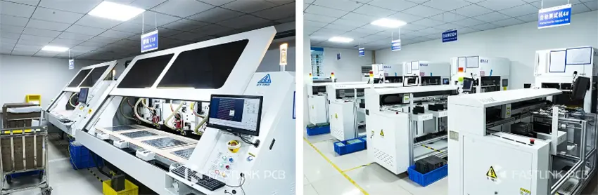
Our 65,000-square-foot state-of-the-art facility in Shenzhen houses the advanced equipment for manufacturing and assembling printed circuit boards. Fastlink leads the industry in quality and performance, whether you need standard fast PCBs or metal PCBs with tight tolerances.
There are more pictures of our factory’s equipment display in our company profile, please click here.
We are duly certified with the following accreditations:
● IATF 16949:2016
● ISO 9001:2015
● ISO14001:2015
● ISO13485:2016
● UL
Furthermore, all our products adhere to the IPC & ROHS Standards. It is our continuous endeavor to produce premium quality PCB products.