- [email protected] Mon-Sun 0. 00-23. 59
When needing prototype printed circuit boards, engaging with a proficient assembler capable of rapidly translating your designs into tangible prototypes is imperative. These boards serve as instrumental tools for verifying the accuracy of your design before initiating a full-scale production, thereby averting expensive errors. The expeditious receipt of your prototype circuit board accelerates the testing phase, propelling you swiftly toward commencing your standard production run.
Our PCB prototype service offered in China stands as one of the quickest and most reliable in the industry. At Fastlink, we boast over a decade of expertise in same-day delivery of operational test models.
To ascertain that the fundamental circuits of your PCB design will operate as envisioned upon assembly, we possess the capacity to deliver a prototype to you in a mere eight-hour span. Printed circuit board prototyping is an essential component of our full-suite, custom-tailored PCB service, serving as a crucial step in preparing your designated circuit designs for a comprehensive manufacturing endeavor.
Every prototyping PCB undergoes a rigorous examination conducted by a flying probe to ensure the connectivity of all vias. Further, to validate the connectivity of all tracks and pads, each PCB is subjected to a 100% Automated Optical Inspection, guaranteeing high precision and reliability.
A Prototype Printed Circuit Board (PCB) is a preliminary version of a PCB design that is fabricated for testing and evaluation purposes. In the electronics design and manufacturing realm, prototypes are crucial as they allow designers and engineers to identify any flaws, inconsistencies, or areas of improvement in the initial design before moving on to mass production. This stage is a cost-effective way to ensure the final product meets the required standards and functions as intended.
The prototype PCB is constructed adhering to the same design specifications as the final product and adjustments may be made following the evaluation of the prototype. The process begins with creating a schematic design, which is then translated into a layout that depicts the positioning of components and the routing of electrical connections. This layout is used to manufacture the prototype PCB. Various testing procedures, including functional testing, are performed on the prototype to validate the design, check for errors, and ensure the circuit performs as required under different conditions.
Moreover, the production of prototype PCBs often utilizes rapid prototyping techniques to speed up the process, which is crucial for meeting project timelines and budgets. This stage also provides an opportunity for stakeholders to make better-informed decisions regarding the design and the manufacturing process, including choices on materials, components, and manufacturing technologies. Besides its technical benefits, prototyping is also advantageous in terms of project management, helping to align expectations, and establishing more accurate timelines and budgets for the entire project.
Prototyping is instrumental in the early detection and correction of errors and issues within the design. By creating a prototype circuit board, designers and engineers can thoroughly inspect and test the circuitry, ensuring it functions as intended. This preliminary step saves significant time and resources by preventing potential errors from being carried into the mass production stage, which would be exponentially more costly to rectify.
A prototype serves as a practical, tangible verification of the design’s functionality. It ensures that all components and circuits operate cohesively and as intended before proceeding to the final production stage. By validating the design early on, it negates the risk of proceeding with a flawed design, ensuring that the final product will function reliably.
The process of prototyping helps in significantly reducing the costs associated with errors that might have otherwise been overlooked. By identifying and rectifying errors in the prototype stage, the costs that would have been incurred in correcting errors during mass production are avoided. Moreover, it prevents the financial and reputational costs associated with product recalls and fixes post-production.
Prototyping accelerates the design process by enabling quick iterations. It allows for timely revisions and corrections of errors, thus shortening the overall time to market. In competitive markets, being able to rapidly transition from design to production can provide a significant advantage.
Prototyping affords designers the opportunity to test different layouts, configurations, and components. It serves as a platform for optimizing the design for better performance, reliability, and manufacturability. Through iterative testing and refinement, the design is honed to its most effective and efficient form.
Prototyping enables the assessment of how different materials affect the performance and functionality of the PCB. It assists in selecting the most suitable materials for the final product, ensuring that the PCB will perform reliably under the intended operating conditions.
1. Design and Schematic Creation: The journey begins with designing the PCB using specialized software. This design not only represents the physical layout but also contains crucial information about the materials, components, and hardware to be used. Once the initial schematic is drafted, it undergoes preliminary checks for defects and simulations to ensure optimal functionality.
2. Bill of Materials (BOM) and Routing Design: The BOM is a comprehensive list detailing every component and material required for production. Concurrently, the routing design is developed, which involves planning the traces that connect each element of the PCB. This phase ensures that power levels, signal noise generation, and other factors are meticulously considered.
3. Comprehensive Design Checks: Before advancing to the fabrication phase, the design undergoes a rigorous examination. This includes checking for thermal issues, conducting design rule checks, and ensuring the layout aligns with the schematic. This step is vital to preemptively identify and rectify potential problems.
4. Photo Film Creation and Inner Layer Printing: Using the finalized design, a photo film of the PCB is produced for each layer. This film guides the subsequent step where copper is applied to the substrate material, followed by a layer of photoresist. The UV-hardened photoresist then reveals the intended copper design.
5. Layer Alignment and Fusion: For multi-layered PCBs, perfect alignment is paramount. Once aligned, the layers are fused together in a process that ensures durability and precision.
6. Drilling, Copper Plating, and Outer Layer Imaging: Precision holes are drilled into the PCB, setting the stage for component placement. The board then undergoes copper plating, ensuring even the interior walls of the drilled holes are covered. An additional layer of photoresist is applied to image the outer layers, solidifying the design.
7. Final Etching and Solder Mask Application: Excess copper is chemically removed, leaving behind the desired conductive connections. The board is then prepared for component attachment with the application of an epoxy solder mask ink.
8. Surface Finish, Silkscreen, and Cutting: A protective layer, often of gold or silver, is deposited as the surface finish. The board’s critical information is then conveyed using ink-jet writing, known as the silkscreen process. Finally, individual boards are precisely cut from the larger panel.
9. Component Sourcing and Assembly: Based on the BOM, all necessary components are sourced. These components are then meticulously assembled onto the board, ensuring each fits perfectly in its designated spot.
10. Soldering, Inspection, and Final Testing: Solder paste stenciling is applied, followed by the placement of surface mount components. The solder paste is then solidified, firmly attaching the components. After reflow soldering, the board undergoes thorough inspections for any discrepancies. The culmination of the prototyping process is a functionality test, simulating real-world conditions to ensure the board’s impeccable performance.
After this rigorous prototyping process, the prototype is tested in real-world conditions. If it meets the desired standards, it paves the way for a full production run, bringing the design to life on a larger scale.
Fastlink stands as one of the leading manufacturers of prototype printed circuit boards, delivering high-quality PCB products to fulfill your project requirements. Whether you need a simple and fast prototype of a printed circuit board, a prototype of an SMT stencil, or a complex placement machine, we can provide it.
With over 10 years of experience in PCB manufacturing and assembly, we hold a unique advantage in rapid printed circuit board prototyping and small- to medium-volume printed circuit board production. Our standard quick turn prototype PCB turnaround time is 1 to 5 days (up to 8 layers).
Our printed circuit boards are used in many industries to power technological advances in electronic devices. The sectors we collaborate with encompass biotechnology, pharmaceuticals, military, medical, food and beverage, laboratory science, microelectronics, aerospace, academia, fuels, petrochemical, chemical, automotive, and power generation.
Through all endeavors, our objective remains unyielding: to shorten the market entry timeline of our client’s products while concurrently enhancing first-time pass rates, safeguarding intellectual property, augmenting product quality, and reducing costs, emissions, and waste.
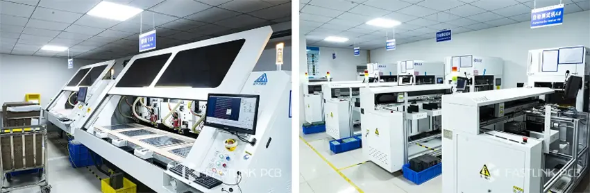
Our 65,000-square-foot state-of-the-art facility in Shenzhen houses the advanced equipment for manufacturing and assembling printed circuit boards. Fastlink leads the industry in quality and performance, whether you need standard fast PCBs or metal PCBs with tight tolerances.
There are more pictures of our factory’s equipment display in our company profile, please click here.
We are duly certified with the following accreditations:
● IATF 16949:2016
● ISO 9001:2015
● ISO14001:2015
● ISO13485:2016
● UL
Furthermore, all our products adhere to the IPC & ROHS Standards. It is our continuous endeavor to produce premium quality PCB products.