- [email protected] Mon-Sun 0. 00-23. 59
Typically, most PCBs are fabricated with copper thicknesses between 1 and 3oz. In contrast, a heavy copper PCB uses copper exceeding 3oz on every layer, encompassing inner and outer layers.
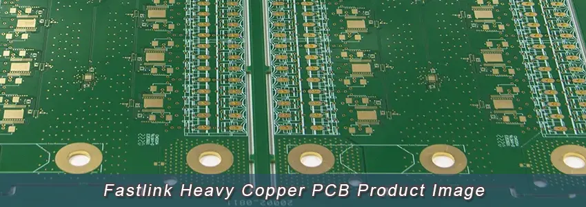
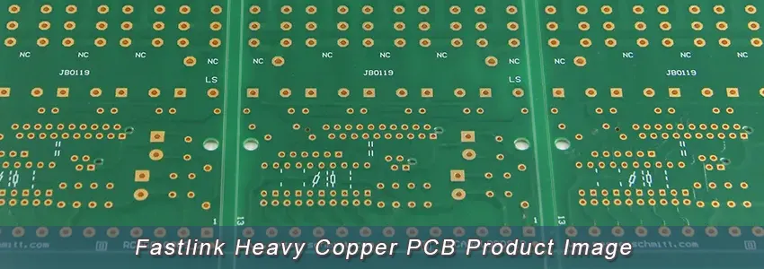
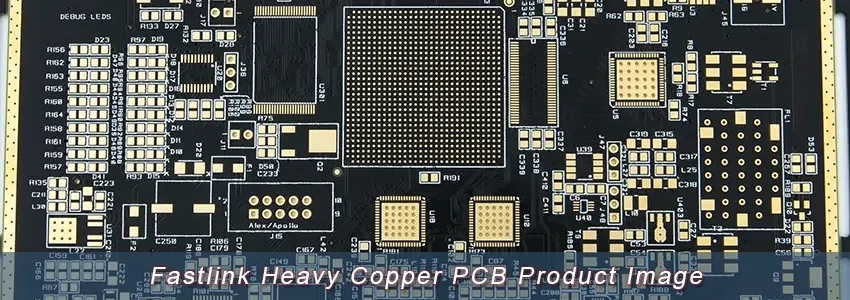
Fastlink is an experienced manufacturer of thick copper PCBs. We design and produce high-quality thick copper PCB products. Our manufacturing capabilities can handle copper weights of up to 15oz (525μm).
1. Increased Current Carrying Capacity: One of the primary reasons for using heavy copper PCBs is the increased current-carrying capacity. Thick copper layers allow for higher currents to pass through the circuit without overheating. This is especially useful for applications that require high-power distribution or high-current operations.
2. Improved Mechanical Strength at Connector Sites: Heavier copper provides added strength at areas where connectors are attached, reducing the risk of damage from mechanical stress, such as when connectors are plugged in and out frequently.
3. Enhanced Thermal Distribution: Heavy copper layers can act as an additional heat sink or thermal plane, helping to dissipate heat away from critical components. This is particularly useful in high-power electronic devices where thermal management is crucial.
4. Increased Durability and Reliability: Thicker copper layers can significantly enhance the lifespan and reliability of the PCB, especially when exposed to harsh environments or when the PCB undergoes a lot of thermal cycling. The PCB is less likely to suffer from issues like circuit breaks or traces lifting off the substrate.
5. Reduced Layer Count: Heavy copper can sometimes reduce the number of layers required in a multi-layer board. By incorporating power and ground planes into a single heavy copper layer, you can achieve what would otherwise require multiple thinner layers.
6. Compact Designs: With the ability to integrate high-current circuits and control circuits on the same board, there’s potential for more compact designs. This is because heavy copper allows for narrow traces that can still carry high currents.
7. High-power and High-thermal Applications: Some applications specifically require heavy copper due to their inherent nature. For example, in power conversion boards, automotive systems, solar power inverters, and military-grade devices, the use of heavy copper is almost a necessity.
A “Copper PCB” typically denotes a board that employs a relatively thin layer of copper to form its circuitry. Standard copper PCBs have thicknesses ranging between 0.5oz/ft^2 and 2oz/ft^2. This measurement, “oz,” signifies ounces per square foot and serves as the metric for copper thickness. Given this configuration, copper PCBs are the mainstay in numerous electronic devices. Everything from our daily-use smartphones, tablets, to laptops integrate these boards. Their manufacturing process is more streamlined due to the thinner copper layers, making them a cost-effective solution suitable for mass production. Primarily, they’re leveraged in applications that necessitate low to moderate power consumption.
“Heavy Copper PCB” is a term reserved for circuit boards that embrace a heftier copper thickness in their conductive layers, specifically starting at 3oz/ft^2 and sometimes even soaring to an impressive 20oz/ft^2. This substantial thickness equips the board to handle considerably larger currents, along with providing stellar thermal performance. Such PCBs are the go-to choice for electronics demanding high power or substantial heat dissipation. We’re talking about intricate power converters, industrial machinery, advanced automotive systems, aerospace equipment, and even military-grade electronics. However, crafting these boards isn’t straightforward. The process of etching such dense copper necessitates specialized techniques, prolonging manufacturing times. This complexity often translates to increased costs. Yet, when one factors in the exceptional capabilities and the longevity these boards offer, especially in high-precision applications, the investment often proves justifiable.
When contrasting Copper and Heavy Copper PCBs, their fundamental divergence lies in the thickness of their copper layers. Standard PCBs hover in the 0.5oz to 2oz range, while their heavy counterparts kick off at 3oz, extending to even greater depths. This difference is not merely cosmetic. The applications of the two are starkly different. Whereas copper PCBs find a home in nearly every conceivable electronic gadget, heavy copper PCBs are reserved for devices and systems where power and heat factors are paramount. Moreover, the cost equation is skewed for heavy copper PCBs due to their intricate manufacturing requirements. Yet, the specific utilities and advantages they usher, especially in niche sectors, often overshadow the initial financial outlay.
Whether double-sided or multilayered, printed circuit boards are fabricated using a blend of copper etching and plating techniques. These circuits begin as slender sheets of copper foil, typically ranging from 0.5 oz/ft2 to 2 oz/ft2. The foil is etched to eliminate unnecessary copper and plated to enhance the copper thickness in areas such as planes, traces, pads, and plated-through holes. Each of these circuit layers is then integrated into a cohesive unit with the help of an epoxy-based substrate, like FR4 or polyimide.
Circuit boards with heavy copper circuits undergo a similar manufacturing process but employ distinct etching and plating methods, including high-speed/step plating and differential etching. In the past, the formation of heavy copper features relied solely on etching thick copper-clad laminated materials. This method often led to uneven trace sidewalls and significant undercutting. However, contemporary advancements in plating technology have facilitated the creation of heavy copper features using a synergistic approach of plating and etching. This results in vertical sidewalls with minimal undercut.
The plating process for heavy copper circuits empowers fabricators to amplify the copper thickness in plated holes and via sidewalls. Today, it’s feasible to amalgamate heavy copper with conventional features on a singular board, a concept referred to as PowerLink. This offers numerous benefits, such as reduced layers, efficient power distribution with low impedance, compact design, and potential cost efficiencies. Conventionally, boards were designed such that high-power/high-current circuits and their corresponding control circuits existed on separate boards. However, with the innovations in heavy copper plating, it’s now achievable to combine these circuits, leading to a board design that’s both compact and straightforward.
Every thick copper PCB we produce is important. Our approach incorporates unique conductive and substrate materials, and our fabrication methods deviate from those employed for standard boards. We use thick copper plating to enhance the copper weight on the sidewalls of vias and plated-through holes, reducing the number of layers. This method permits the seamless integration of high-current and control circuits, thus creating high-density boards even with streamlined board structures.
In conventional subtractive manufacturing, etching thick copper PCBs often leads to the challenge of undercutting, resulting in copper traces having a trapezoidal cross-section instead of the desired rectangular one. To address this, Fastlink employs an additive manufacturing approach. We methodically build the selected thick copper layers through this technique via a specialized plating process.
1. Copper Thickness: The copper thickness is chiefly determined by the current passing through the conductor. A trace width calculator could be utilized to ascertain the copper thickness by evaluating parameters like trace width, current capacity, and temperature rise.
2. Heat Dissipation and Thermal Strains: Heavy copper PCBs are known for their enhanced heat dissipation capabilities, which is vital in enduring the recurring thermal cycles that occur during fabrication and assembly processes. This increased endurance to thermal strains is a notable benefit.
3. Mechanical Strength: The mechanical strength at connector sites and in plated-through holes (PTH) is significantly increased in heavy copper PCBs. This attribute is crucial for applications that demand robust connections and durability.
4. Current Carrying Capacity: The amount of current a copper circuit can safely carry is dependent on the heat rise the project can withstand, as there’s a direct relationship between heat rise and current flow. The IPC formula can be employed to model the heat rise associated with the applied current, aiming for a stable operating temperature where heating equals cooling.
5. Reduced Product Size and Layer Count: Incorporating multiple copper weights on the same layer of circuitry can lead to a reduction in the product size. Additionally, the integration of heavy copper with standard features on a single board, known as PowerLink, can lead to reduced layer count, smaller footprints, and potential cost savings.
6. Design for Manufacturing (DFM): DFM is critical in heavy copper PCB design, encompassing considerations like line width and line space which are vital for successful manufacturing.
7. Placement of Heavy Copper: Determining where heavy copper is needed is crucial. Analysis of the circuit and thermal requirements helps in determining the optimal placement of heavy copper, ensuring that thicker copper is allocated only in areas that will benefit, thus avoiding unnecessary cost escalations.
8. Line Width: Minimum line width is a crucial consideration and is often one of the first questions asked of a PCB manufacturer’s capabilities. The answer to this largely depends on the copper weight.
1. Heavy Machinery: Heavy copper PCBs are crucial components in heavy machinery such as transformers, motors, and generators. They facilitate optimal energy transmission, thereby improving operational efficiency and minimizing energy wastage.
2. Military Applications: Within the military sector, heavy copper PCBs find use in weapons control systems, radar, and monitoring systems. Their ability to handle high currents and provide efficient thermal management makes them suitable for these critical applications.
3. Automotive Industries: The automotive sector employs heavy copper PCBs in rail track systems and signal transmission systems. These PCBs can withstand the high-temperature and high-power conditions often encountered in automotive applications.
4. Industrial Equipment: Heavy copper PCBs are often utilized in industrial, automotive, or military equipment that requires high-power or high-temperature tolerance.
5. Power Electronics: In power electronics, heavy copper PCBs are commonly used in motor drives, power supplies, and inverters. They can handle high currents, making them suitable for high-power applications, and provide efficient thermal management, which is crucial for the reliable operation of power electronic devices.
| Feature | Parameters |
| Material | FR4, Aluminum, Ceramic, Special Board Materials: Rogers, Teflon, Polyimide, Copper core. |
| Quality class | IPC 2/IPC 3 |
| Thickness of copper | 2oz-20oz |
| Extremely heavy copper | 20oz-200oz |
| Layers | 2 – 18 layers |
| Build Time | 3 – 10 working days |
| Delivery time | 5 days – 2 weeks |
| Max Outer Copper Weight (Finished) | 20oz |
| Maximum inner layer copper weight | 12oz |
| Type of hole | Via/Blind Via/Buried Via |
| Via Coverage | Via Tent / Via Plugging / Via Fill |
| Surface treatment | ENIG/OSP/HASL/IAG/ISN/ENEPIG/ ROHS |
| Minimum Solder Mask Distance | 6mil |
| Solder Mask Color | Green/White/Blue/Black/Red/Yellow/ Purple/Matte |
| Minimum silkscreen line width | 8mil |
| Silkscreen Color | White/Yellow/Blue/Black/Red |
| Smallest ring | 6mil |
| Minimum drilling diameter | 10mil |
| Impedance control | +/-5%~10% |
| Board outline | Punching, Routing, V-Cut |
Having amassed extensive expertise in PCB production technology over the years, Fastlink is adept at manufacturing heavy copper PCBs with an inner layer copper thickness ranging from 0.5oz to 12oz and an outer layer copper thickness spanning from 3oz to 20oz. Should you require heavy copper PCBs, we stand as your trustworthy partner.
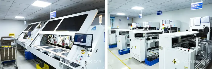
Our 65,000-square-foot state-of-the-art facility in Shenzhen houses the advanced equipment for manufacturing and assembling printed circuit boards. Fastlink leads the industry in quality and performance, whether you need standard fast PCBs or metal PCBs with tight tolerances.
There are more pictures of our factory’s equipment display in our company profile, please click here.
We are duly certified with the following accreditations:
● IATF 16949:2016
● ISO 9001:2015
● ISO14001:2015
● ISO13485:2016
● UL
Furthermore, all our products adhere to the IPC & ROHS Standards. It is our continuous endeavor to produce premium quality PCB products.