- [email protected] Mon-Sun 0. 00-23. 59
Rigid PCBs are a fine choice if you seek a circuit board solution that is economical and conducive to large-scale production. Their durability often surpasses that of other boards, such as flexible PCBs, making them a robust selection for those seeking a hard-wearing circuit board. The enhanced circuit density of rigid PCBs further underscores their suitability for demanding applications.
Rigid circuit boards are popular in products and industries where components must remain fixed, as they can withstand high temperatures and pressures throughout their operation.
Fastlink, a leading supplier of rigid printed circuit boards, manufactures rigid boards to your exact project requirements. The materials and configurations we use ensure that your rigid PCBs operate reliably in different environments while maintaining good durability.
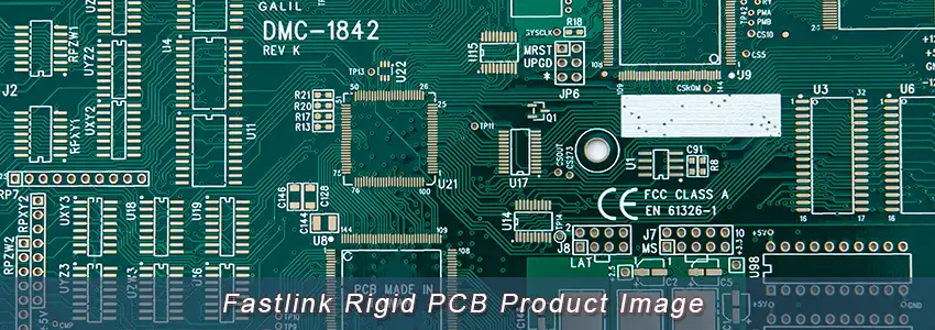
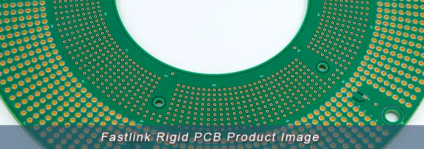
A rigid PCB is a solid and inflexible type of PCB that can be single-sided, double-sided, or multilayer. Once manufactured, rigid PCBs cannot be modified or folded into other shapes. They comprise several material layers, such as a substrate layer, a copper layer, a solder mask layer, and a silkscreen layer, which are bonded together using adhesive and heat. Rigid PCBs are the most common type of PCB, and examples include computer motherboards and mobile phone PCBs.
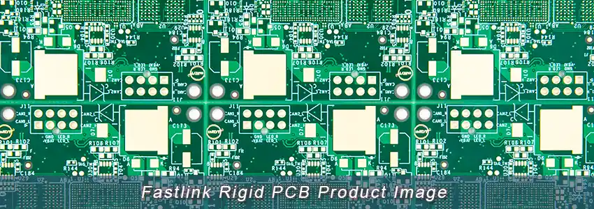
The construction of a rigid circuit board entails a solid substrate adorned with copper tracks and designated component layouts. Active and passive electronic components (whether Through-Hole, SMD Components, or a Mixed PCB Assembly) are affixed upon these layouts, typically employing automated soldering technologies. The soldering processes may encompass Hole Soldering Technology such as Wave Soldering, Automated Surface Mount Technology (SMT) like Reflow Soldering, or even manual Hand Soldering when necessary.
1. Single-sided: The archetype of PCBs, single-sided circuit boards, possess a singular layer of conductive material, with all components arrayed on one side. Their simplistic design expedites manufacturing, minimizing error probabilities. With their capability to excel in low-density designs, these cost-effective configurations are a staple in the industry.
2. Double-sided: Unlike their single-sided counterparts, double-sided PCBs harbor copper conductive layers on both surfaces, doubling the components’ real estate. This design amplification augments circuit complexity and diversifies design possibilities, rendering them suitable for a broad spectrum of projects.
3. Multilayer: This type of PCB employing three or more conductive layers ensconced amidst several insulating layers obviates the necessity for interconnection wiring. Through advanced curing processes, these multilayer boards conserve space, engendering a compact, robust PCB capable of handling intricate circuitry.
Rigid PCBs, often called PCBs, are the conventional type of circuit board commonly envisioned when thinking of circuit boards. They comprise electrical components connected through conductive tracks and other elements on a non-conductive substrate. The substrate in a rigid PCB usually incorporates glass to reinforce the board, providing strength and rigidity. This structural firmness offers excellent support for components and decent thermal resistance, making rigid PCBs a reliable choice for various electronics applications.
On the other hand, flexible PCBs differ by featuring a flexible base material like polyimide instead of a rigid substrate. This flexibility enables them to withstand vibrations, efficiently dissipate heat, and be folded into multiple shapes, suiting them for compact and innovative electronics. The unique attribute of flex circuits comes from their ability to flex, which is crucial for modern electronics that require adaptability in form and function. Their structural adaptability makes them a preferred choice for applications demanding resilience and compactness.
Besides the base layer material and rigidity, other distinctions exist between rigid and flexible PCBs. For instance, flexible circuits often employ more adaptable rolled annealed copper as the conductive material to accommodate bending, unlike the electro-deposited copper used in rigid PCBs. The manufacturing process also varies; flexible PCBs utilize an overlay or overlay process to shield the exposed circuitry instead of the solder mask used in rigid PCBs. Although flex circuits may have a higher upfront cost than rigid PCBs, their ability to fit into compact spaces reduces product size, leading to indirect savings and justifying the cost difference.
The manufacturing process of rigid PCBs begins with a detailed design and layout phase, which is crucial for ensuring the functionality and reliability of the final product. In this phase, engineers use computer-aided design (CAD) software to create a precise blueprint of the PCB. This design specifies the location and orientation of all components, traces, vias, and other crucial elements. It also includes information about the layers of the PCB, which is critical for multi-layer boards. Once the design is finalized, it is converted into a format that can be used by the manufacturing machinery, often using a Gerber file or similar.
The core material for rigid PCBs is usually a fiberglass substrate, like FR4, which provides the required structural rigidity. The material is cut into panels of the required dimensions in preparation for the manufacturing process. A copper foil is then laminated onto one or both sides of the fiberglass substrate, depending on the design specifications. This copper layer will later be etched to create the electrical connections between components.
The image transfer stage involves applying a layer of photoresist material to the copper-coated substrate. This photoresist is sensitive to ultraviolet light. The board is then exposed to ultraviolet light through a mask that carries the desired pattern. Where the light hits the photoresist, it hardens; where the mask blocks the light, the photoresist remains soft and can be washed away, revealing the copper beneath.
After the image transfer, the exposed copper is etched away using a chemical etchant, typically a solution of ferric chloride or ammonium persulfate. This process removes the unwanted copper, leaving behind the copper traces that form the circuit pathways. The remaining photoresist is then stripped away, leaving a clean and precise copper pattern.
Drilling is the next step, where holes are drilled into the PCB for through-hole components and vias. The accuracy of the drilling is crucial for ensuring proper alignment and functionality. Automated drilling machines are used to achieve the high level of precision required, and the drill data is taken directly from the PCB design files to ensure accuracy.
The holes and traces are then electroplated with a thin layer of metal, usually copper, to ensure good electrical conductivity throughout the board. This step can also include the application of a solder mask over the copper traces to protect them and prevent solder bridging during the assembly process.
A solder mask is applied to the board to cover everything except the pads where components will be soldered. This mask helps prevent accidental connections (shorts) between copper traces during the soldering process. It’s a crucial step for ensuring the reliability of the PCB.
Silkscreen printing is done next, where identifying information like component labels, company logos, and other necessary markings are printed onto the solder mask. This step helps technicians place components correctly during the assembly process and provides a professional finish to the PCB.
A surface finish is applied to protect the copper traces and ensure good solderability. Common surface finishes include Hot Air Solder Leveling (HASL) or Electroless Nickel Immersion Gold (ENIG). This step is crucial for ensuring the long-term reliability and performance of the PCB.
After the surface finish is applied, the PCBs are subjected to a range of tests to ensure they meet the specified design criteria. Automated Optical Inspection (AOI) and Electrical Test (E-test) are commonly used to check for defects such as shorts, opens, or incorrect component placements. Any defects identified at this stage can either be repaired or, if irreparable, the boards are discarded.
In this stage, the boards are profiled to their final shape, and V-cuts may be made to allow for easy separation of multiple boards that were manufactured as a panel. This is often done using CNC machines or laser cutting, based on the specifications and tolerances required.
A final inspection is carried out to ensure all quality standards have been met, and the PCBs are free from defects. Once approved, the PCBs are packaged carefully to prevent damage during transit and are then shipped to the customer or moved to the next stage of assembly. This final step ensures that the product delivered meets the high-quality standards required in the electronics industry.
The assembly process for rigid PCBs involves multiple steps. Each step requires precision and attention to detail to ensure a high-quality, reliable finished product.
Prior to assembly, a Bill of Materials (BOM) is prepared, listing all the components required for the PCB. This includes the type, value, quantity, and location of each component. The BOM is crucial for procurement and inventory management, ensuring that all necessary materials are available for assembly.
Once the BOM is prepared, the required components are procured. This step may involve sourcing parts from multiple suppliers to ensure quality and cost-effectiveness. It’s essential to verify the components’ accuracy and authenticity to ensure the assembled PCB’s reliability.
The PCBs are inspected for any defects that might have occurred during the manufacturing process. This includes checking for scratches, shorts, or any other physical or electrical anomalies. Automated Optical Inspection (AOI) or X-ray inspection can be used for this purpose.
A stencil is prepared based on the PCB design, and solder paste is applied to the board using this stencil. The solder paste is applied only to the areas where components will be mounted. This is a crucial step as the amount and placement of solder paste will significantly affect the soldering quality.
Automated machines pick components from the feeders and place them on the PCB in the designated locations as per the design files. The precision and speed of the pick-and-place machines are crucial for ensuring accurate component placement and optimizing production time.
The boards, with components placed, are then sent through a reflow oven. The heat in the oven causes the solder paste to melt and form solid connections between the components and the PCB. The reflow process has to be carefully controlled to avoid solder bridges or cold solder joints.
For any through-hole components or components that could not be placed by the automated machines, manual insertion is done. Skilled technicians place these components by hand.
The boards are then sent through a wave soldering machine, which solders the leads of the through-hole components to the board. Alternatively, selective soldering can be used to solder specific areas of the board.
After soldering, the boards are cleaned to remove any residual solder flux or other contaminants. This step is crucial for ensuring the long-term reliability of the PCB.
Once cleaned, the boards undergo a secondary inspection to check for any soldering defects, misaligned components, or other issues. Functional testing, In-Circuit Testing (ICT), or Flying Probe Testing can be performed to verify the functionality and electrical performance of the board.
A final inspection is carried out to ensure that all issues have been addressed and the boards meet the quality standards. This may include a visual inspection, AOI, X-ray inspection, and additional functional testing.
1. Consumer Electronics: Rigid PCBs are extensively used in consumer electronics such as smartphones, tablets, laptops, televisions, and gaming consoles. They provide the necessary platform for mounting and interconnecting the electronic components that drive these devices.
2. Automotive Industry: Modern vehicles heavily rely on electronics for various functionalities like engine control units, airbag systems, navigation, audio systems, and many others. Rigid PCBs are used to host and connect these electronic components in a reliable and durable manner.
3. Industrial Applications: In industrial settings, rigid PCBs find applications in control systems, automation equipment, and power distribution boards among others. They can withstand the harsh conditions often present in industrial environments.
4. Medical Devices: Medical devices such as imaging systems, monitors, and control systems in medical equipment heavily depend on rigid PCBs. They ensure the reliability and precision required in medical electronics.
5. Aerospace and Defense: Rigid PCBs are used in avionics, radar systems, control systems and other critical electronic systems in aerospace and defense applications. The reliability and durability of rigid PCBs are crucial in these sectors where failure is not an option.
6. Telecommunications: The telecommunications sector relies on rigid PCBs for routers, switches, and other networking equipment. They provide the necessary infrastructure for the complex circuitry involved in data transmission and reception.
7. Computing: Computers and servers are another major application area for rigid PCBs. They host the processors, memory, and other critical components that are integral to the operation of computing systems.
8. Renewable Energy Systems: Rigid PCBs are used in the controllers and inverters of solar and wind energy systems. They play a crucial role in the efficient conversion and management of energy in renewable energy systems.
9. Lighting: In modern lighting systems, especially LED products, rigid PCBs are used to provide electrical connections and mechanical support for the light-emitting diodes.
10. Security Systems: Electronic security systems such as surveillance cameras, alarms, and access control systems also employ rigid PCBs to ensure reliable operation.
11. Smart Home Technologies: With the advent of smart homes, rigid PCBs are being used in smart thermostats, lighting controls, and other home automation gadgets.
| Items | Mass | Prototypes |
| Layers | 1-30 Layers PCB(FR4) 1-4 Layer PCB(Ceramic) 1-4 Layer PCB( Metal Core) | 1-34 Layers PCB(FR4) 1-6 Layer PCB(Ceramic) 1-6 Layer PCB( Metal Core) |
| Max. Panel Size | 600*770mm( 23.62″*30.31″) | 600*770mm (23.62″*30.31″) 500*1200mm (19.69″*47.24″) |
| Max.Board Thickness | 8.5mm | 8.5mm |
| Min. Board Thickness | 2L:0.3mm | 2L:0.1mm |
| 4L:0.4mm | 4L:0.3mm | |
| 6L:0.8mm | 6L:0.6mm | |
| Min Inner Layer Clearance | 3mil | 3mil |
| Min Line width | 3/3 mil | 3/3 mil |
| Min Line space | 3/3 mil | 3/3 mil |
| Min.Hole Size | 0.1mm | 0.1mm |
| Min plated hole thickness | 25um | 25um |
| Min Blind/Buried hole size | 0.1mm | 0.1mm(1-18layers) |
| PTH Dia. Tolerance | ±0.076mm(±3mil) | ±0.076mm(±3mil) |
| Non PTH Dia. Tolerance | ±0.05mm(±2mil) | ±0.05mm(±2mil) |
| Min S/M Pitch | 0.1mm (4mil) | 0.1mm (4mil) |
| Soldermask colour | Green,black, Blue,White, Yellow,Red | Green,black, Blue,White, Yellow,Red |
| Silkscreen colour | White,Yellow, Red,Black | White,Yellow, Red,Black |
| Outline | Routing,V-Groove, Beveling punch | Routing,V-Groove, Beveling punch |
| Outline Tolerance | ±0.15mm ±6mil | ±0.15mm (±6mil) |
| Peelable mask | Top,bottom, double sided | Top,bottom, double sided |
| Controlled Impedance | +/- 10% | +/- 7% |
| Through Hole Resistance | <300Ω(Normal) | <300Ω(Normal) |
| Electric Strength | >1.3KV/mm | >1.4KV/mm |
| Peel Strength | 1.4N/mm | 1.4N/mm |
| Solder Mask Abrasion | >6H | >6H |
| Flammability | 94V-0 | 94V-0 |
Fastlink specializes in turnkey PCB fabrication and assembly services, offering high-quality, low-cost, and fast delivery to customers worldwide. With 15 years of industry experience in complex multilayer PCB processing, partnering with us significantly mitigates your risk. We continuously invest in innovation, production equipment, and engineering expertise to enhance our technological capacity and capabilities. We offer high-quality rigid PCBs at competitive prices.
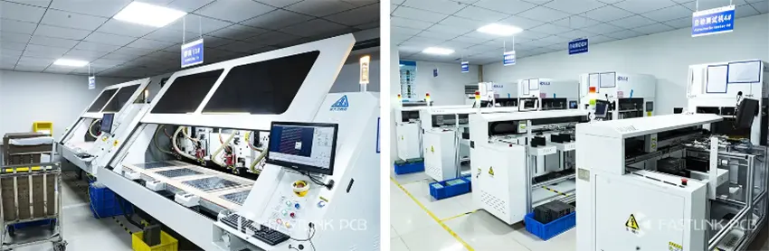
Our 65,000-square-foot state-of-the-art facility in Shenzhen houses the advanced equipment for manufacturing and assembling printed circuit boards. Fastlink leads the industry in quality and performance, whether you need standard fast PCBs or metal PCBs with tight tolerances.
There are more pictures of our factory’s equipment display in our company profile, please click here.
We are duly certified with the following accreditations:
● IATF 16949:2016
● ISO 9001:2015
● ISO14001:2015
● ISO13485:2016
● UL
Furthermore, all our products adhere to the IPC & ROHS Standards. It is our continuous endeavor to produce premium quality PCB products.