- On November 17, 2025
- In blog
PCB Surface Mount Technology: Reflow Soldering
Reflow soldering is the most crucial step in PCB assembly, often seen as the “finishing touch.” By carefully controlling the heating process, it permanently bonds the solder, components, and the circuit board, ultimately determining the electrical performance and mechanical reliability of the final product. This article will provide an overview of the basic principles and key steps involved in reflow soldering. We will also discuss common soldering defects in PCB production, their underlying causes, and offer practical solutions and preventive measures.
What is Reflow Soldering ?
Reflow soldering is a method used in Surface Mount Technology (SMT) to connect electronic components to printed circuit boards (PCBs). The process works by heating the solder paste to a high temperature, causing it to melt and form a strong bond with the component leads and PCB pads as it cools. This ensures reliable electrical contact, contributing to the durability and performance of the connection.
1. Applying Solder Paste
First, solder paste, a mixture of metal alloy particles, flux, and other additives, is applied evenly to the pads of the circuit board. Solder paste serves as the medium to connect the components to the PCB and will melt during the heating process to form reliable solder joints.
2. Placing Components
Next, electronic components such as chips or other surface-mount devices are precisely placed on the solder paste-covered pads according to the design specifications. This is typically done using a custom stencil, which accurately transfers the paste onto the pads through openings that match the PCB layout, ensuring the paste is applied evenly and components are positioned correctly.
3. Reflow Soldering
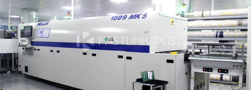
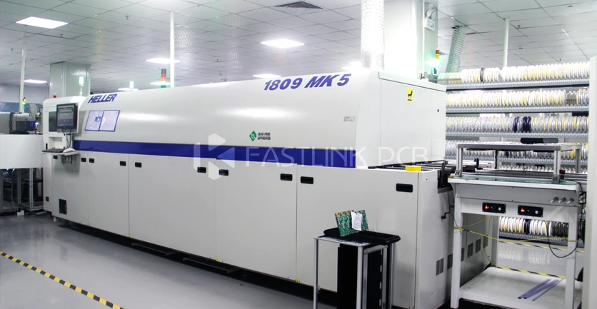
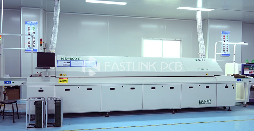
Reflow soldering consists of four key temperature zones that follow a specific sequence: the preheat zone, soak zone, reflow zone, and cooling zone. Each zone has its specific role, with different temperature settings.
A.Preheat Zone
In the preheat zone, the temperature is usually set between 60°C and 130°C. This stage allows the PCB and components to gradually heat up. If the temperature increases too quickly, thermal shock could damage the components and PCB. Preheating helps avoid this, while also allowing moisture and volatile substances in the solder paste to evaporate, which reduces the formation of bubbles in the solder joints and prepares everything for the next soldering stages.
B.Soak Zone
The soak zone typically ranges from 120°C to 160°C. At this stage, the goal is to ensure the PCB and components reach a uniform temperature, fully evaporating any remaining moisture. This step prepares the system for the reflow zone and prevents thermal shock, which could lead to defects.
C.Reflow Zone
The reflow zone is the most crucial part of the process. Here, the temperature quickly rises to about 245°C. At this temperature, the solder paste melts, flowing and spreading between the PCB pads and component leads, completely filling the solder gaps.
It’s important to note that the reflow oven temperature is adjusted based on the melting point of the solder paste. For instance, low-temperature solder paste melts around 138°C, so the oven temperature is set to approximately 180°C±5°C. Medium-temperature paste melts around 178°C, requiring the oven to be set at about 215°C±5°C. High-temperature paste melts at 217°C, so the oven temperature is set to 245°C±5°C. In general, the oven temperature is slightly higher than the melting point of the solder paste.
D.Cooling Zone
In the final cooling zone, the temperature is rapidly reduced to allow the solder to solidify, creating a strong solder joint. The cooling process needs to be carefully controlled to avoid thermal stress from a rapid temperature change, which could impact the quality of the solder joints.
How to Avoiding Reflow Soldering Pitfalls ?

Reflow soldering involves many factors, including the accuracy of solder paste printing, component placement, and the precise control of the oven temperature profile. Each step requires careful attention to detail. In manufacturing, different stages of the process often lead to specific soldering defects, such as solder balls, tombstoning, and solder bridging. Identifying the root causes of these defects and implementing effective solutions, while also preventing them during production to avoid risks, is essential for improving product yield and quality.
1. Solder Ball Defects
Solder balls are usually caused by incomplete melting and bonding of the solder paste between the component leads and the PCB pads. Poor wetting can cause the molten solder to shrink unevenly, resulting in migration and the formation of scattered spherical solder balls instead of smooth, complete solder joints. The primary cause is often insufficient wetting.
How to Prevent It?
- Ensure Cleanliness and Accurate Printing of the PCB: Before reflow soldering, make sure the PCB is clean. Any printing misalignment or solder paste residue can cause defects.
- Optimize Stencil Design: A poorly designed stencil with unclear openings can lead to excessive solder paste or bridging, especially for fine-pitch components.
- Watch the Solder Paste Shelf Life: If solder paste sits for too long after printing, it can oxidize, losing its activity. It’s recommended to use solder paste with a shelf life of at least 4 hours.
- Control the Temperature Profile Carefully: A low peak temperature or insufficient reflow time can prevent the solder paste from melting fully. If the preheating phase is too fast, solvents may not evaporate properly, causing solder balls to scatter. A heating rate of 1–4°C per second is recommended.
2. Tombstoning Effect
Tombstoning, or the “Manhattan effect,” occurs when one end of a surface-mount component lifts during reflow, typically due to uneven heat distribution. For example, when one side of the component reaches the solder melting point (around 183°C) first, the solder melts, and the surface tension pulls the other side up.
How to Prevent It?
- Proper Preheating: Insufficient preheating, especially in processes like vapor phase soldering, can cause thermal imbalance. It is recommended to preheat components to 145–150°C and hold for 1–2 minutes.
- Design Pads Correctly: Asymmetrical or oversized pads can lead to uneven solder paste distribution and differences in thermal absorption. Pad designs should follow IPC standards closely to ensure balanced heat distribution.
3. Solder Bridging in Fine-Pitch Components
Solder bridging between fine-pitch leads is a common and serious defect, typically caused by mismatched design or process parameters.
How to Prevent It?
- Ensure High-Quality Solder Paste: Unstable viscosity or inconsistent metal content can increase the likelihood of bridging. Use high-quality solder paste and ensure proper storage conditions.
- Precise Printing and Placement: Misalignment during printing, excessive solder paste, or improper placement pressure can result in short circuits. Accurate control of the printing position and placement height is essential.
- Adjust Reflow Temperature Settings: Rapid heating can increase the risk of bridging. The temperature profile should include adequate preheating and dwell time to avoid this issue.
4. Other Common Reflow Soldering Defects
- Porosity/Pinhole Defects: These are caused by the rapid evaporation of solvents or moisture during the soldering process. To address this, ensure the solvents fully evaporate during preheating, or increase the solder paste’s viscosity and metal content.
- Insufficient Solder: This occurs when the wetting is poor, or the solder paste is insufficient. To solve this, improve the wettability of the pads and components, or use a flux with higher activity.
- Component Shifting: This is often caused by uneven solder paste thickness, poor placement accuracy, or uneven heat distribution. Improving placement accuracy, standardizing pad sizes, and adjusting the oven temperature profile can prevent this.
- Poor Wetting: The main causes are poor wettability of the pads or components, insufficient flux activity, or inadequate heating. Increasing the peak reflow temperature or using a more active flux can help improve wetting.
- Dull and Rough Solder Joints: These are typically related to contamination or vibration during the cooling stage. Avoiding disturbances during cooling and adjusting the cooling rate can help improve joint appearance.
- Void Formation: Voids occur when gas trapped inside the solder joint cannot escape, weakening the connection. Improving preheating and increasing solder paste viscosity can help with venting and reduce voids.
- Cold or Weak Joints: These defects often arise when the pads and leads are not aligned properly (co-planarity issues) or when there are significant differences in thermal mass. To address this, improve component coplanarity, increase solder paste thickness, balance heat transfer, or adjust the solder alloy to delay melting.
Final Thoughts
To sum up, the quality of the reflow soldering process directly impacts the final performance and reliability of PCB assemblies. By thoroughly understanding the process and meticulously controlling each stage, we can minimize defects and ensure product quality.
At Fastlink, our advanced reflow soldering equipment and experienced process experts have made excellent process control a standard part of our production. This is why we have earned the trust of many customers as their preferred manufacturing partner. If you have any questions about reflow soldering or PCB assembly, our team is always available to offer professional and timely support.
