
- On August 11, 2026
- In blog
What Is PCB Routing?
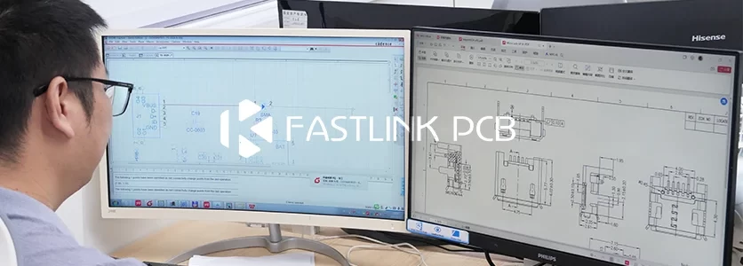
If a PCB is envisioned as a miniature electronic metropolis—with ICs and discrete components acting as its buildings—then PCB routing is the design and construction of its physical highway network.
In essence, routing is the critical phase during layout where abstract schematic netlists are transformed into real copper traces on the board. Far from simply “connecting the dots,” modern PCB routing is a multidisciplinary engineering discipline that balances electrical performance, thermal dissipation, and physical stackup rules to guarantee both optimal signal integrity and high yield during manufacturing.
What is PCB Routing?
Every well-designed trace serves three core functions:
- Signal Transmission: Providing precise, unimpeded paths for high-speed data signals.
- Power Delivery: Delivering stable electrical energy across components to satisfy specific current demands.
- Return Path Provision: Creating continuous, low-impedance return channels for current to eliminate EMI and signal attenuation at the source.
In practice, engineers must carefully manage trace geometry and routing topology. Key parameters include trace width and spacing to balance current capacity with safety clearance, layer-to-layer via transitions, and controlled impedance alongside length matching for high-speed interfaces like DDR, PCIe, USB4, or SerDes.
Additionally, differential pairs demand tightly coupled parallel routing to minimize skew, while high-current power networks rely on wide traces, heavy copper pours, and stitching vias to achieve low-inductance connections.
Modern PCB layout methodologies leverage a combination of manual routing, interactive push-and-shove tools, auto-routing algorithms, and AI-assisted routing strategies. The ultimate objective is ensuring long-term, reliable system operation while adhering strictly to layer stackup rules, mechanical boundaries, and electrical constraints.
Routing Methodologies
Fundamentally, all PCB routing involves laying copper conductors across outer and inner layers to establish physical connections between components. However, even simple component interconnects can demand vastly different routing strategies depending on electrical requirements. Whether routing low-frequency control lines or ultra-high-speed data lanes, layout engineers must account for several critical design factors:
- High Current & Power Distribution: Standard fine traces cannot support high amperage without overheating. Power networks require significantly wider traces, copper pours, or dedicated polygon planes to minimize thermal buildup and voltage drop.
- Routing Topology: Selecting the proper layout topology—such as point-to-point, daisy-chain, or star routing—determines how efficiently a net distributes signals across multiple load nodes.
- Signal Loss & Length Constraints: Dielectric and conductor attenuation limit maximum routing distances. Total insertion loss budgets dictate how far a high-frequency signal can travel before requiring re-drivers or signal conditioning.
- Timing & Skew Control: In parallel buses, differential pairs, and synchronous interfaces using SPI or I2C, arrival timing skew must be tightly constrained. Layout tools apply serpentine length matching to ensure signals land within specified phase windows.
- Trace Geometry & Clearances: Minimum trace widths and spacing parameters govern fabricator yield, while enforcing clearance rules—is vital for suppressing adjacent line crosstalk.
- Controlled Impedance Modeling: Signal lines requiring specific target impedances must have trace widths and dielectric clearances engineered precisely against the physical layer stackup.
FastlinkPCB’s Role in PCB Routing Optimization
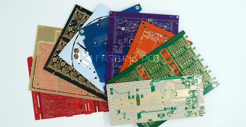
PCB routing is ultimately an engineering balance between electrical performance, signal integrity, and physical manufacturing constraints. Translating an optimized routing design into a reliable physical board requires precise execution on the factory floor. Drawing on extensive manufacturing experience, FastlinkPCB provides:
- DFM Optimization & Risk Mitigation: Identifying potential layout bottlenecks during pre-production to streamline routing layout and downstream SMT assembly.
- Manufacturing-Grade Routing Precision: Enforcing tight control over trace width tolerances, etch compensation factors, and via plating thickness to match target impedance specs.
- High-Speed & High-Power Tailoring: Fine-tuning trace geometries and copper weight distribution based on substrate dielectric properties and thermal dissipation demands.
- Automated DRC & Design Verification: Running thorough automated DRC inspections prior to tooling to detect and correct micro-clearance violations or manufacturing risks.
Partner with FastlinkPCB
Backed by automotive and industrial-grade fabrication capabilities, advanced production equipment, and comprehensive DFM support, FastlinkPCB transforms your layout into high-yield, reliable hardware. Contact the FastlinkPCB engineering team today to request a DFM review or quote for your next PCB project.