
- On September 30, 2026
- In blog
How Much Does a Custom PCB Cost?
If you have requested fabrication quotes recently, you may have noticed a stark discrepancy between pricing today and quotes issued just a few months ago. This upward shift is very real.
Since late 2025, the PCB manufacturing sector has undergone a major wave of price adjustments. The primary driver is the relentless cost inflation of Copper Clad Laminates —driven by simultaneous price surges across copper foil, woven glass cloth, and epoxy resin systems. As a result, standard laminate raw material costs have escalated 30% to 50% compared to early-year baselines.
Compounding this raw material inflation, the explosive growth in AI server infrastructure has prompted tier-1 fabricators to allocate substantial factory capacity toward high-density, high-layer-count products, squeezing lead times and capacity for conventional rigid PCBs. Combined with localized supply chain disruptions in high-performance resin systems, fabrication lead times have stretched, driving cost pressure directly down to end customers.
This guide breaks down the key price determinants—layer count, substrate selection, board dimensions, production volume, and specialized surface finishes—to help you optimize procurement decisions in the current market environment.
What Factors Affect Custom PCB Cost?
Layer
Among the many variables that influence custom PCB manufacturing costs, layer count is the single most critical baseline factor. Virtually all downstream fabrication, material, and processing costs scale directly from the board’s structural layer configuration.
Layer count serves as the primary driver of fabrication overhead. Adding layers increases raw material consumption, requires additional lamination cycles, extends drilling time, and introduces complex registration and inspection steps. Crucially, fabrication cost does not scale linearly: a 4-layer PCB typically costs 2.5 to 3 times more than a standard 2-layer board, rather than simply double.
The relative cost multiplier across standard layer counts generally follows this progression:
| Layer | Relative Cost (2L = 1.0) |
| 1L | 0.7x |
| 2L | 1.0x(baseline) |
| 4L | 2.5–3.0x |
| 6L | 4.0–5.5x |
| 8L | 6.0–8.5x |
| 10+ L | 10–20x |
Order Quantity
Alongside layer count, production volume is one of the most decisive variables in custom PCB pricing.
The Prototyping Premium: Non-Recurring Engineering Costs
Why are prototype unit costs so much higher than volume production runs? Manufacturing the initial prototype panel incurs significant upfront non-recurring engineering expenses. These setup costs cover CAM engineering review, photolithography tooling, stencil fabrication, lamination thermal cycle setup, and CNC drill programming. Because these overhead expenses are fixed, they apply equally whether producing a single board or a run of 100 panels.
Unit Cost Scaling
As order quantities scale, fixed setup and tooling fees are amortized across a larger volume of units. Consequently, marginal production costs are reduced to raw substrate consumption and machine run time:
10 to 100 Units: The sharpest drop in unit pricing occurs within this range, often yielding a 50% to 60% reduction in per-board cost.
Exceeding 1,000 Units: The cost curve flattens as NRE and setup fees become fully diluted. At this scale, raw material consumption (CCL laminates, copper foil) and automated assembly machine time dictate the baseline unit price.
When structuring a custom PCB budget, consolidating procurement orders or scaling up initial build quantities significantly optimizes unit economics and overall ROI.
Panel Dimensions
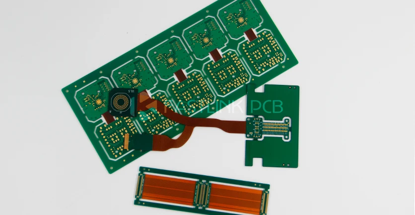
The next critical variable is board size. While physical dimensions appear to be a straightforward matter of surface area, their true impact on manufacturing costs involves panel yield dynamics.
Fabrication pricing generally scales with total board surface area, but the relationship is non-linear. Production lines operate using standardized master production panels—typically 18″ × 24″ (457 mm × 610 mm) or 21″ × 24″ (533 mm × 610 mm)—onto which individual PCBs are arrayed. Because raw substrate material is billed at the full panel level, unutilized border space and poor nesting geometry directly drive up the effective cost per square inch.
DFM Tip: For small-form-factor boards, optimize panel utilization by supplying or requesting a custom panelization array (using V-scoring or tab-routing with mouse bites). The minor tooling and depaneling fees are almost always outweighed by the raw material savings gained from eliminating scrap waste on master panels.
Substrate Material
Substrate material selection is a primary determinant of baseline PCB manufacturing costs. Standard FR-4 offers the most economical cost-to-performance ratio, serving as the industry default for standard consumer and industrial electronics.
However, when designs demand elevated thermal endurance, low-loss high-frequency signal integrity, or enhanced heat dissipation, material costs increase exponentially. For instance, substituting standard FR-4 with Rogers RO4350B on a 4-layer PCB architecture can increase total fabrication costs by 5x to 6x. This price differential reflects the high raw material procurement costs and specialized processing parameters (such as tight dielectric thickness control and modified lamination cycles) associated with high-frequency RF laminates.
| Substrate | Relative Cost |
| FR-4 (Tg 130–140°C) | 1.0x |
| Tg FR-4 (Tg 170–180°C) | 1.2x – 1.5x |
| Aluminum | 2.0x – 4.0x |
| Rogers 4000 | 4.0x – 6.0x |
| Polyimide / Flex | 5.0x – 10.0x |
| Rogers RT | 8.0x – 12.0x |
| Ceramic-Filled PTFE | 10.0x – 20.0x |
Surface Finish
The primary function of a PCB surface finish is to prevent copper pads from oxidizing while establishing a solderable interface for downstream SMT assembly. Surface finishes differ significantly in process execution overhead, bare-board shelf life, coplanarity, and overall cost.
Avoiding Unnecessary Surface Finish Costs
For approximately 90% of standard rigid PCB designs, conventional leaded or HASL provides a durable, cost-effective solution.
Upgrading to ENIG—which typically carries a 20% to 40% premium over standard HASL—is generally justified under two specific DFM conditions:
Fine-Pitch Components: The layout incorporates fine-pitch BGAs, CSPs, or QFNs with pad pitches of ≤20mil, where absolute pad coplanarity is required to prevent solder bridging or open joints.
Extended Shelf Life: Bare PCBs require an extended shelf life exceeding 12 months before undergoing SMT reflow or hand assembly.
For designs utilizing standard passive chip components (e.g., 0805 / 0603 footprints), discrete semiconductors, or standard QFP ICs, standard HASL delivers optimal solderability without the added cost of noble metal finishes.
Copper Thickness
The industry baseline for standard PCB fabrication is 1 oz finished copper weight. Specifying heavy copper incurs a notable price premium. Thicker copper foils demand extended chemical etching cycles, increase undercutting risks, and restrict the minimum achievable trace width and spacing tolerances.
| Copper Thickness | Relative Cost |
| 0.5 oz | -10% – 20% |
| 1.0 oz | Baseline |
| 2.0 oz | +15% – 30% |
| 3.0 oz | +30% – 50% |
| 4.0 oz or more | +50% – 100%+ |
DFC Strategy
Upgrading an entire board stackup to 2 oz copper simply to accommodate one or two high-current power traces creates unnecessary cost overhead.
1.Solder Mask Openings: Maintain a standard 1 oz finished copper baseline across the board. For high-current traces, remove the solder mask over those specific copper paths. During wave soldering or SMT assembly, add solder paste or solder-bonded copper jumper bars along the exposed trace to increase cross-sectional area and current-carrying capability.
2.Asymmetrical Heavy Copper Stackup: If heavy copper is structurally required, specify 2 oz copper strictly on outer layers while maintaining standard 1 oz copper on inner signal layers. This asymmetrical approach fulfills surface thermal and current demands without inflating inner-layer etching, drilling, and lamination processing costs.
Lead Time
The standard lead time for volume PCB fabrication typically spans 10 to 15 business days. When turnaround times are compressed, the factory must reprioritize production queues, schedule overtime shifts, and interrupt standard automated line scheduling—generating substantial expediting surcharges.
| Fabrication Lead Time | Relative Cost |
| 10–15 Business Days | 1.0× (Baseline Cost) |
| 5–7 Business Days | +20% – 40% |
| 3–4 Business Days | +50% – 80% |
| 24–48 h | +100% – 200% |
Advance Planning Is the Best Way to Save Money
In product development, optimizing project schedules to align with standard production lead times is the single most effective DFC (Design for Cost) strategy.Same-day or 24-hour express turnarounds operate on “firefighting” pricing models. For non-critical production runs, paying a $2\times$ to $3\times$ cost premium yields poor ROI. Reserving 1 to 2 weeks for standard fabrication turnaround completely eliminates expediting surcharges, keeping your overall unit economics on target.
How to Reduce the Total Cost of Ownership for Custom PCBs?
Achieving optimal cost performance for custom PCBs requires moving beyond factory fabrication fees alone. Total cost of ownership must be managed holistically across four key pillars: component procurement, SMT assembly, system architecture, and R&D design.
- Component Sourcing & Supply Chain Risk Management
Direct component substitution yields immediate BOM savings, but requires rigorous qualification:
Mitigate Obsolescence Risks: Avoid specifying EOL or NRND components, which risk supply chain bottlenecks and force costly board re-spins.
Verify Environmental Operating Limits: Low-cost second-source alternatives may meet nominal specifications at room temperature, but suffer parameter drift under thermal stress or supply rail variations.
Procure via Authorized Distributors: Source strictly through franchised distributors or franchised brokers to avoid gray-market counterfeit ICs or reclaimed silicon.
- Design for Manufacturability & PCBA Optimization
For volume production, SMT machine placement time and manual labor constitute major overhead. Implementing DFM best practices directly reduces assembly costs:
Standardize on Surface Mount Components: Eliminate through-hole components where possible, as SMDs enable fully automated high-speed SMT placement without manual insertion steps.
Enforce Single-Sided Placement: When board real estate permits, locate all SMT components on a single primary side. This limits assembly to a single stencil and one reflow soldering pass, saving tooling fees and thermal cycle costs.
Minimize High-Density Package Types: Avoid BGAs, CSPs, or bottom-terminated QFNs unless strictly necessary. Fine-pitch packages require automated X-ray inspection and tight process controls; lower yield rates on these packages increase overall scrap costs.
Specify Automated Packaging Feeder Formats: Order components on tape and reel or matrix trays rather than loose cut-tape, avoiding manual feeder loading fees during pick-and-place setup.
- System Architecture & Hardware/Software Partitioning
Analog vs. Digital Partitioning: Re-evaluate fundamental circuit topologies. For instance, determine whether a threshold-detecting circuit is best handled by an integrated ADC on a microcontroller or an inexpensive discrete comparator IC, matching performance to actual tolerance requirements.
Software-Defined Hardware Offloading: Shift hardware functionality into firmware algorithms. For example, implementing button debouncing in software eliminates RC filter networks and hardware gates.
Deploy Pre-Certified RF Modules: For Wi-Fi, Bluetooth, or cellular IoT designs, utilize fully integrated, pre-certified modules such as FCC or CE compliant units. While module BOM costs are slightly higher, they bypass regulatory RF compliance testing fees.
- Engineering Efficiency & Rapid Time-to-Market
For low-to-medium volume builds, initial NRE, prototyping, and engineering labor dominate total project expenditure:
Leverage Reference Topologies: Implement vendor datasheet reference designs and proven in-house sub-circuits to minimize prototyping iterations and layout errors.
Design with Strategic Performance Margins: For low-volume products, selecting slightly higher-spec components to eliminate custom tuning circuits saves substantial engineering evaluation time and yields lower overall total cost.
Get Your Custom PCB Quote Today
While global PCB manufacturing regions offer distinct localized advantages, China remains the primary supply chain partner for the majority of global electronics projects—offering mature ecosystem integration, highly competitive cost structures, and dependable manufacturing quality.
As highlighted in the opening section of this guide, raw material markets remain volatile. Key laminate inputs—including copper-clad laminates and copper foil—continue to face upward pricing momentum, causing fabrication quotes to vary over short timeframes. For active design projects, locking in volume pricing and factory line capacity early is essential to mitigate material inflation and protect project budgets.
If you are evaluating custom PCB fabrication, contact FastlinkPCB. Our engineering team provides transparent, competitive quotations tailored to your Gerber files, stackup requirements, order volumes, and fabrication tolerances—helping you optimize manufacturing costs in today’s dynamic market.