- On May 28, 2025
- In blog
A Comprehensive Guide to Choosing PCB Inspection
Why is PCB inspection so important? Because defective printed circuit boards can have dire consequences in terms of cost and brand reputation. In industries such as medical and automotive, where human life is at stake, the consequences can be even more severe.
For this reason, PCB inspection has become an integral part of the manufacturing process. To ensure stable performance throughout the circuit board’s life cycle, the industry has developed a variety of inspection methods, ranging from basic visual checks to more complex structural testing. Each method has its own application scenario.
This article will introduce you to several mainstream methods of inspecting PCB quality. Whether you work in manufacturing or are simply interested in the electronics industry, we hope this content will help you to gain a better understanding of PCB quality control.
Common PCB Inspection Methods
1.Manual Visual Inspection (MVI)
The most basic PCB inspection method is manual inspection. The operator, through the naked eye or using a magnifying glass, compares the PCB with the design documents under a magnified view, looking for common defects such as solder joint problems, device offsets, empty welds, broken wires, burrs, and so on.
This method is low cost and fast, and is suitable for boards with simple structures or small production runs. However, for PCBs with hidden solder joints or densely packed components, manual inspection is prone to missing problems, and the accuracy depends on the operator’s experience.
2.Automatic Laser Measurement (ALT)
ALT is a high-precision inspection method based on laser scanning, which is mainly used to measure the quality of solder paste printing, the height of solder joints and the reflection characteristics of components. It can quickly analyze whether the distribution of solder paste is uniform, whether there is any offset or omission, and effectively improve the controllability of the assembly process. Although ALT has high inspection speed and accuracy, it may be interfered when components are obscured.
3.X-ray Inspection (AXI)
For modern high-density PCBs using packages such as BGA, CSP, etc., it is difficult to “see” whether the hidden solder joints are reliable or not with conventional inspection methods. X-ray inspection can penetrate the package, from the internal observation of the structure of the solder joints, to identify the solder ball hole, false soldering, bridging and other hidden problems. Due to the relatively high price and cost of X-ray inspection equipment, it is not necessary to use for simple circuit boards without chip packages.
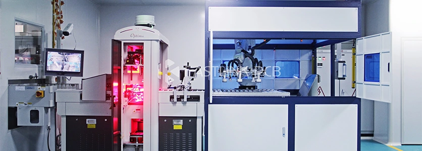
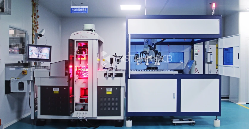
4.Automatic Optical Inspection (AOI)
Automatic Optical Inspection is the more advanced and efficient alternative to MVI. It uses multiple high-definition cameras and light sources to capture PCB images from multiple angles and compare them with standard templates to identify problems such as scratches, knots, stains, thinned solder, open circuits, short circuits, misplaced or missing components.
Modern AOI is divided into 2D and 3D versions, the latter can also accurately measure component height and deformation, for three-dimensional structure of the more complex circuit boards to provide higher inspection accuracy. the advantages of AOI is fast, repeatable, suitable for mass production of the quality control link, but the disadvantage is that it is still not able to check the package internal solder joints. Therefore, AOI can not be the only inspection method, it needs to be applied in conjunction with other inspection methods.
How to Choose the Right PCB Inspection Method?
In circuit board manufacturing, choosing the right inspection method usually requires comprehensive consideration from the following dimensions:
1.Complexity
The more complex the structure of the circuit board, the higher the requirements for inspection accuracy. For simple single-sided PCBs, the traditional manual visual inspection can usually meet the needs of low-cost and easy to operate. For double-sided or multilayer PCB, many key solder joints and lines can not be directly observed with the naked eye, which requires the use of more advanced detection methods in order to effectively identify internal defects.
2.Production Batch
Production scale is also an important reference when choosing inspection methods. High-volume production projects are more suitable for the deployment of automated inspection systems, such as AOI or multi-functional sensor equipment, which can improve inspection efficiency and reduce human error. For small lot sizes or prototyping, manual or semi-automated inspection methods can be considered to save upfront investment while maintaining flexibility.
3.Project Budget
Budget constraints can directly affect the range of technologies available. Manual visual inspection is cheaper, but has limited detection capability to cover all hidden defects. Technologies such as X-ray inspection, 3D AOI or ALT laser measurement offer higher inspection accuracy and data visualization capabilities, but the equipment investment is relatively high.
4.The Quality Requirements of the Industry
Different industries have different quality tolerances for PCBs. For example, the consumer electronics industry pcb can accept a certain range of small deviations, but medical device pcb, aerospace or new energy vehicles and other areas of high reliability requirements, often require a higher level of inspection system for the gatekeeper, even if the circuit board structure is not complex, but also to meet the strict standards.
FastlinkPCB Uses Top Tier PCB Inspection to Rout Defects
At FastlinkPCB, we always adhere to a rigorous quality management system and continue to invest in advanced PCB inspection and test equipment. Currently, we are equipped with multiple AOI systems and X-ray inspection equipment, which can efficiently identify all kinds of soldering defects and hidden problems. At the same time, we have an experienced quality inspection team, which can combine the equipment data with the actual process to provide professional inspection guarantee for each circuit board.
FastlinkPCB is committed to providing one-stop PCB solutions from manufacturing, assembly to inspection. Whether it’s a prototype trial or a large-volume delivery, we can achieve consistent quality. If you are looking for a PCB manufacturing partner with professional inspection capabilities and industry experience, please feel free to contact FastlinkPCB.