- [email protected] Mon-Sun 0. 00-23. 59
As electronic products become smaller and faster, problems such as signal interference, delay and system instability, which were previously only encountered in high-end equipment, are now also beginning to appear in ordinary circuit design. Many engineers have found that, even at low frequencies, circuits can have a variety of ‘invisible’ problems that are often not taken into account in High speed PCB design.
In fact, high speed PCB technology is no longer specific to a single industry; it is a fundamental requirement for the majority of modern electronic products. Understanding the principles of high speed PCB design and manufacturing can help you avoid many potential problems.
Many people think that only boards with a frequency of 50 MHz or higher are high speed PCBs, but this is not the case. High speed PCBs do not have a fixed frequency limit; rather, it is a judgment based on the actual situation. The key is whether the signal speed is fast enough to affect the circuit’s impedance characteristics or component performance or cause signal radiation, skin effect, dielectric loss, and other phenomena. If any of these conditions are met, the board should be considered High speed.
Since these terms are often used interchangeably, people often wonder if high speed and high frequency PCBs are the same. In fact, there is no significant difference between the two.”high speed” and “high frequency” emphasize different concepts. “High speed” emphasizes completing the level conversion in a very short period of time, while “high frequency” refers to a signal with a higher oscillation frequency. However, in PCBs, High speed and high frequency often occur simultaneously because high frequency signals require a shorter period. This naturally requires the rise/fall time of the signal to be very fast, exhibiting High speed characteristics.
In short, most high frequency signals are High speed signals. Therefore, High speed and high frequency PCBs have similar materials, design priorities, and manufacturing requirements. There is no strict boundary between the two; often, they can be understood as different expressions of the same type of PCB. Therefore, we do not need to be overly concerned with their names; what is important is maintaining the integrity and stability of High speed signals in the circuit.
A high speed PCB requires a reasonable layout and wiring, as well as the right materials to meet the strict impedance, signal integrity, and electromagnetic compatibility requirements of High speed signals. This chapter will introduce you systematically to the key points of high speed PCB design from three core aspects.
1.The layout of a PCB is its foundation, determining the signal path and power distribution of the entire board. An effective layout can reduce signal reflection, crosstalk, and delay while optimizing power integrity. The following recommendations should be kept in mind when designing high speed PCBs:
2.Maintain the minimum aspect ratio:The recommended aspect ratio for through-holes is 1:10, and the recommended aspect ratio for microvias is no greater than 1:0.75. This ensures the quality and reliability of the hole walls.
3.Use microvia technology to reduce plate thickness:Microvia technology effectively reduces plate thickness and is suitable for the compact layout of high speed signals.
4.Control the number of laminations:The continuous lamination process should not exceed three times. More than five to six times may cause process problems and affect the quality of the finished product.
5.Prioritize back-drilling when connecting a large number of blind holes:Using back-drilling reduces lamination, drilling, and filling cycles, improving production efficiency.
6.Copper Thickness and Line Width Matching:The line width should be 3 mils. The copper thickness should begin at 9 microns to ensure conductivity.
7.Pay attention to the impact of complex components: Complex components, such as BGA package density and spacing, determine the number of stacked PCB layers. A targeted design should be used for different pitch BGAs.
After completing the layout, the next critical aspect to guarantee signal integrity is cabling design. Since High speed signals require precise wiring, length matching, and differential pair design, refer to the following points:
The preferred option is a four-layer board structure. One layer should be dedicated to a continuous, complete ground layer. The other inner layer should be a power layer to reduce impedance. Place High speed components close to the ground layer using microstrip technology with wires. If double-sided boards are necessary due to cost constraints, set up the signal line on both sides of the ground copper area. Use dense over-hole stitching technology to firmly connect them and form an effective low-impedance return path. Strictly avoid crossing the two sides of the high speed line.
Arbitrary placement of signaling vias can create voids in the power or ground plane, forming “hot spot” areas. Placing the vias in a grid at regular intervals and maintaining proper spacing helps maintain an even distribution of current.
90-degree turns are prone to signal reflections and impedance surges and do not allow for fine etching. 135-degree or rounded corners are designed to guide signals more smoothly.
High speed signals that are too close to each other due to electromagnetic coupling cause crosstalk. Whenever possible, increase the spacing between neighboring alignments, especially outside dense alignment areas.
Keep the spacing between differential pairs constant and avoid placing vias, capacitors, or pads in between to maintain consistent differential impedance. Coupling capacitors and vias should be placed symmetrically.
High speed interfaces, such as DDR, USB, and PCIe, have extremely high signal synchronization requirements. Ensure that positive and negative signals, or multiple signals, arrive at the same time using serpentine alignment.
When wiring analog and digital signals on the same board, try to isolate the regions and avoid crossing each other’s ground layer.
During the design phase, the analog and digital areas should be divided into functional zones to ensure that components and alignments are in the correct zones, thus avoiding unnecessary cross-wiring and interference coupling.
The component pin or pad size should be as close as possible to the calculated ideal alignment width to prevent sudden changes in impedance at the connection between the pad and the alignment and maintain signal continuity.
The performance of a high speed PCB depends not only on the layout and wiring, but also on the choice of material, as it directly affects the speed and quality of signal transmission. Due to the high frequency and even microwave signals in high speed PCB design, the performance of common FR-4 no longer meets the demand.
1.Dielectric Constant (Dk): affects the speed of signal transmission and impedance characteristics. If the dielectric constant of the high-speed material does not match then it may lead to circuit signal failure.
2.Dissipation Factor (Df): indicates the energy loss of a signal as it travels through the material. Like the dielectric constant, a mismatched dissipation factor has a significant effect on the transmission of the circuit signal.
3.Coefficient of Thermal Expansion (CTE): Determines the thermal stability of the material. We should make sure that the CTE between different substrates in the manufacturing process match each other to ensure the reliability of the PCB when the temperature rises. Note that the expansion rate of XYZ direction need to be concerned.
4.Thermal Coefficient of Dielectric Constant (TCDk): This represents the degree of change in dielectric constant with temperature, generally the more stable the better.
5.Thermal conductivity: this affects the thermal performance, in some applications that require high heat dissipation should be considered in order to ensure that the device works stably.
6.Conductive Anode Filament (CAF) Control: CAF is a common failure mechanism, usually caused by metal migration, which may lead to circuit shorting. In order to reduce this risk, priority should be given to the use of high-quality copper foil materials with good CAF resistance.
7.Mechanical Strength Requirements: the product should be in the design stage to fully consider the manufacturing feasibility and its performance in the actual application environment, such as electromagnetic interference (EMI), electromagnetic compatibility (EMC), signal reflection, thermal cycling, vibration, flexible strain and mechanical shock. For the scene emphasizing physical stability, the mechanical properties of the material should be considered as an important basis.
8.Cost: Although high-speed PCB materials compared to ordinary materials cost more, but in most application scenarios, this investment is worthwhile. Select the right material not only improve performance, but also significantly reduce the risk of rework later.
Two of the most important properties are Dk and Df. According to signal loss characteristics, high speed PCB materials can be divided into four categories:
1.Normal Speed and Loss Materials
FR-4 materials belong to this category and are suitable for digital and analog circuits within a few GHz. However, their dielectric constant and loss with frequency changes are more obvious, which limits their performance in high speed applications.
| Std Loss High Speed Material | |||||
| Halogen-free | EM370(5) | EM285 | TU-747HF1 | IT150G | NPG-170N |
| Halogenated | IT-180A | TU-768 | S1000-2 | NP175F | EM-825 |
2.Medium-Speed, Medium-Loss Materials
This type of material has a smooth change in dielectric constant with frequency. The loss is approximately half that of ordinary materials. It is suitable for applications up to about 10 GHz.
| Mid Loss High Speed Material (0.020) | |||||
| Halogen-free | H175HF | EM828G | EM370(D) | Megtron2 | IT170GT |
| Halogenated | S7038 | IT2OOLK | TU862S/T | IS415 | FR408 |
3.High speed, Low-Loss Materials
These materials have a smooth dielectric constant frequency response and low signal loss. They are suitable for high frequency, high speed circuits.
| Low Loss High Speed Material (0.012) | |||||
| Halogen-free | EM-526 | EM-888 | H180HF | TU-863+ | EM-888K |
| Halogenated | S7439 | M4/M4S | IT-958G | I-Speed | IT200LK |
4.Very High Speed, Very Low Loss Materials (RF/Microwave Materials)
These materials have an extremely flat dielectric constant frequency response and the lowest losses. This makes them suitable for microwave and RF applications up to 20 GHz and even higher frequencies.
| Ultra Loss High Speed Material (0.004-0.008) | ||||
| Halogen-free | TU883/SP | Synamic6 | EM-528 | NPG-170N |
| Halogenated | Tachyon 100G | TU933E | IT968/SE | MW1000/2000/3000/4000 |
In high speed PCB design, there is little room for error. Even if the design is perfect, a tiny error in the manufacturing process can greatly reduce the performance of a board. The value of a one-stop service lies in the fact that we will take care of every step of the process, from high speed PCB design and testing to manufacturing.
Before entering production, potential problems must be identified through electromagnetic and signal integrity simulations. Tools such as SPICE, Ansys HFSS, and Cadence can help designers optimize the alignment, impedance configuration, and thermal distribution layout before real manufacturing.
Unlike standard PCBs, high speed PCB boards have more stringent manufacturing requirements regarding frequency, impedance, thermal management, and other factors. Therefore, manufacturers must have greater manufacturing precision.
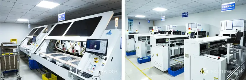
There are more pictures of our factory’s equipment display in our company profile, please click here.
FastlinkPCB is a professional high frequency/high speed PCB manufacturing expert with over 15 years of experience in the industry, specializing in meeting the needs of demanding high frequency applications.

Contact us in the lower right corner for reliable high speed PCB solutions.