
- On October 20, 2026
- In blog
Overview of Hot Swap PCB Solutions
As a manufacturer specializing in high-precision circuit board fabrication and surface mount assembly, we encounter diverse hot-swappable architecture designs across our daily production lines:
Enthusiast and Low-Volume Custom Builds: Widespread utilization of Mill-Max pin receptacles, delivering exceptional tactile insertion feel and robust mechanical stability for mechanical keyboards.
Mass Consumer and Gaming Peripherals: Extensive implementation of standardized hot-swappable switch sockets such as Kailh, balancing high manufacturing throughput with competitive unit economics.
Professional Office and Split Ergonomic Keyboards: Integration of rigid-flex PCB technology, enabling complex folding geometries or modular split-board layouts.
Portable Gaming and Wireless Devices: Direct on-board integration of low-energy Bluetooth and proprietary radio frequency wireless modules to support seamless, low-latency connectivity anywhere.
What is a Hot-Swap PCB?
Simply put, a hot-swap PCB is a circuit board that allows on-board components to be replaced at any time without requiring a soldering iron for re-soldering.
In the field of mechanical keyboards, this design enables users or engineers to freely replace switches, LED diodes, or stabilizers. You only need to pull out the part and insert a new one to complete the replacement immediately, making the whole process time-saving and effort-saving.
To achieve this convenient solderless experience, we need to add dedicated sockets during the circuit design stage.
From the perspective of manufacturing and structure, the core of achieving stable hot-swapping lies in the following key elements:
- Precision Metal Sockets: This is the core component for securing component pins. The inside of the socket features high-elasticity metal contact spring clips that tightly clamp the inserted switch pins.
- Reliable Electrical Contacts: When the switch is inserted into the socket, the contacts seamlessly complete the circuit. This way, every time a user presses a key, the electrical signal can be transmitted quickly and stably.
- Mechanical Latching and Retention Structure: Beyond electrical connections, the socket itself needs to possess sufficient mechanical gripping force. This prevents keys from loosening or falling off during frequent keystrokes or transport bumps.
- High Interface Compatibility: An excellent PCB design needs to be compatible with mainstream switch pin configurations on the market (such as 3-pin or 5-pin switches) to ensure the board can adapt to the vast majority of standard switches.
For PCB manufacturers, hot-swapping is not as simple as adding a socket. Controlling solder pad strength during surface mount production to ensure sockets do not desolder or fail after thousands of insertions and removals is the real key to determining product quality.
Manufacturing Process of Hot-Swap PCBs
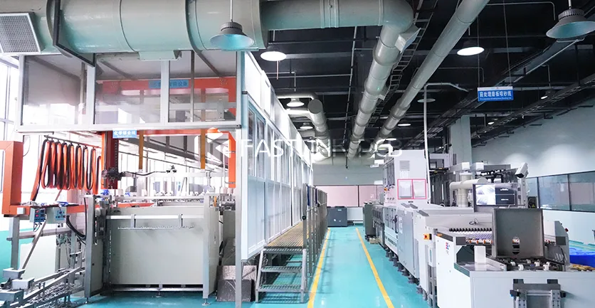
Building a hot-swappable printed circuit board with both high stability and excellent tactile feel relies not only on circuit design, but also on quality control at the factory end.
1.Precision Lamination, Etching, and High-Precision Drilling
Conventional hot-swap pcb mostly adopt a double-sided board structure. Although the layer count is not high, the requirements for machining precision are extremely high.
Switch socket and positioning hole tolerances: The mounting holes and pin positions of hot-swappable switch sockets must be extremely precise. Even a minute deviation of 0.2 millimeters will cause the switch socket to misalign or make the switch impossible to insert.
High-density multi-layer hot-swappable board application: If your hot-swappable printed circuit board integrates red green blue lighting effects, a microcontroller unit, and radio frequency or bluetooth wireless modules, we usually recommend upgrading to a 4-layer board. Dedicated power layers and ground layers can provide stable power supply for red green blue lamp beads, and can also effectively reduce electromagnetic interference, making layout in the dense microcontroller unit routing area smoother.
2.Surface Finish Processes and Surface Mount Assembly
Choosing the appropriate surface finish method directly determines the soldering strength and durability of the hot-swappable sockets.
Hot air solder leveling: Cost-effective, suitable for early simple test samples or budget-sensitive projects.
Electroless nickel immersion gold: Extremely flat surface, an excellent choice for hot swap pcb. It can ensure the flatness of surface mount pads, significantly improving the peel strength and contact reliability of hot-swappable switch socket pads.
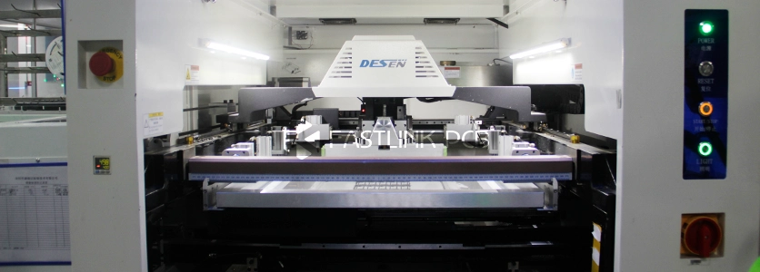
Surface mount placement material preparation optimization: When performing hot-swappable printed circuit board assembly contract manufacturing, advance confirmation of inventory for hot-swappable switch sockets such as Kailh or Gateron, diodes, and red green blue lamp beads is crucial to prevent delivery delays caused by parts shortages.
3.Comprehensive Inspection
In the pre-shipment testing stage, we always control quality from the perspective of the end user’s actual usage experience:
Key matrix circuit test: 100% electrical testing passed to ensure every matrix line of the hot-swappable printed circuit board is clear, eliminating short circuits and open circuits.
Switch socket insertion and extraction force actual measurement: Practical measurement of switch installation through manual or mechanical means to ensure hot-swappable switch sockets are neither loose nor require hard forcing to insert, with no risk of pad detachment.
Red green blue lighting effect consistency check: One-by-one screening of surface mount lamp beads to ensure no dead lights, color casting, or uneven brightness.
Enclosure interference verification: Precisely checking the board edge outline, positioning holes, and universal serial bus port positions of the hot swap pcb to ensure the circuit board can perfectly fit into your structural enclosure.
Why Are Hot-Swap PCBs Important?
Nowadays, hot-swap designs are no longer an “optional feature” within enthusiast circles, but a standard requirement for the vast majority of custom and commercial keyboards.
For PCB manufacturers, this means that switch socket footprint design, substrate structural strength, switch compatibility, and factory testing standards must all be executed according to stringent industrial-grade production specifications.
For keyboard designers and brand owners, selecting the right switch socket and surface finish process in the early stages of circuit board design directly determines the long-term reliability of the product in users’ hands.
To give a very practical example: in a mass production run of 10,000 hot-swap PCBs, downgrading the surface finish from electroless nickel immersion gold to hot air solder leveling can indeed save $0.50 to $1.00 per board, which looks like an upfront savings of $5,000 to $10,000.
However, in actual use, frequent switch insertion and extraction by users leads to solder pad peeling. Once the pad detachment rate spikes from 0.5% to 5%, for keyboards priced between $80 and $150, the resulting product returns, customer support repairs, and brand reputation losses will instantly wipe out all the profits saved upfront.
This trade-off between cost and quality must be calculated clearly during the circuit board design and material selection stages, rather than waiting until post-sales returns pile up high before trying to fix it.
Ready to Start Your Next Hot-Swap PCB Project?
As a manufacturing team focusing on high-precision circuit board and PCB assembly processing, FastlinkPCB possesses mature hot-swap PCB surface mount processes and a rigorous design for manufacturability evaluation system. We can provide you with professional engineering support during the prototyping and volume production stages!