- On February 5, 2026
- In blog
PCB Reverse Engineering: Compliance, Workflow, and Technical Barriers
PCB reverse engineering involves much more than just copying; it is a sophisticated process of data extraction and reconstruction. Using advanced inspection techniques, engineers convert physical circuit boards into editable digital design files. This article provides an objective analysis of PCB reverse engineering, covering its benefits, legal compliance, workflows, and technical hurdles.
The Purpose and Benefits of PCB Reverse Engineering
PCB reverse engineering solves real problems in industrial settings, which is why many companies treat it as a go-to tool. A common use case is analyzing critical boards when the design package is missing or the documentation is outdated. Done well, it helps keep production reliable and supports the development of newer versions that run better and cost less to build.
Rebuilding Design Data for PCBs With No Documentation
Most modern PCB projects come with solid CAD files and supporting technical documentation. But boards can change hands, move across teams, or sit in storage—and the original files sometimes disappear along the way. When that happens, reverse engineering becomes the practical way to recover the schematic and the key design details. It also rebuilds the product documentation, so engineering teams can handle repairs or produce copies without working blind.
Keeping Mission-Critical Boards Running
Legacy PCBs often handle essential jobs like supplying power to equipment or driving electronic components. If one of these boards fails, finding a replacement can be tough, and technicians may not have any usable reference materials. Reverse engineering addresses both issues. It gives engineers what they need to support long-term maintenance, and when repair isn’t possible, it also enables board cloning to produce a functional replacement.
Cutting PCB Manufacturing Costs
When a competing product is priced unusually high, reverse engineering can help estimate what it likely costs to make. In markets with little competition, selling prices often sit far above actual manufacturing expense. Once a company understands the cost breakdown, it can release a comparable product at a more reasonable price point. That move can bring in customers who previously had no viable alternative.
Relying Less on Outside Specialists
When a board fails, many companies turn to outside experts. The problem is that specialists with the right niche background aren’t always available. That gap in expertise can stall production. Reverse engineering provides the board’s underlying technical information, which helps internal teams pinpoint the fault area on their own instead of waiting for external support.
Finding Weak Spots in Competitor Designs
PCB manufacturers constantly look for ways to improve efficiency. Reverse engineering a competitor’s product can reveal exactly where the design falls short. Engineers can take those findings and improve their own circuitry to deliver better performance in the market. And even when sales isn’t the goal, users can still benefit—by identifying weaknesses and building a more efficient custom solution for a specific application.
PCB Reverse Engineering Compliance: Is Cloning a Board Legal?
Developers keep coming back to the same question: Is it legal to copy a PCB? With PCB Reverse Engineering, there isn’t a single yes-or-no answer. Intent matters, and local law matters even more. That’s why nobody in the industry can honestly hand out a blanket “legal” or “illegal” verdict.
When PCB Reverse Engineering Is Commonly Defensible
There are a few scenarios where PCB Reverse Engineering is often treated as reasonable—and sometimes protected:
- Repair and maintenance: If an OEM has dropped support, engineers may reverse a board to keep equipment alive. Think about it—if the machine is mission-critical, “sorry, no longer supported” doesn’t fix anything. This is where the “right to repair” idea usually applies.
- Education and research: If someone is studying circuit principles for teaching or academic work, that typically lands in fair use territory. The focus is learning, not competing in the market.
- Interoperability: Sometimes PCB Reverse Engineering is about compatibility, not cloning. Why? Because customers expect products to work together. A straightforward example is a third-party charging cable designed to work with existing devices.
Where PCB Reverse Engineering Gets Risky
Here’s where engineers and companies can get burned:
- Patents: “Redrawing the layout” isn’t a magic shield. If the circuit design or logic is patented, selling something that uses that protected design can still be infringement—even if the PCB artwork looks different.
- Trade secrets and NDAs: How the board was obtained is a big deal. If it was stolen, or if someone breaks an NDA to do PCB Reverse Engineering, trade secret law can come into play quickly.
- Copyright and 1:1 cloning: PCB routing and layout can be treated like creative expression. A physical 1:1 clone made to profit commercially is the kind of move that invites serious legal trouble.
Practical Advice Before Selling Anything
If a business wants to commercialize a design that comes out of PCB Reverse Engineering, it should bring an IP attorney in early—before production decisions get locked in. And on the engineering side, aim for real transformation, not surface-level tweaks. Make the “new” design meaningfully different, and the risk of disputes drops fast.
Types of PCB Reverse Engineering
Engineers don’t pick a PCB Reverse Engineering method at random. Two questions drive the decision: How replaceable is the sample? And how close does the final data need to be? Answer those, and the path usually becomes clear.
Destructive Reverse Engineering (DRE)
DRE is the classic “peel the onion” approach. The technician images a layer, then removes material, then images the next layer—repeat until the stack is gone. This is typically done with precision milling gear or controlled board-grinding tools. Sure, someone can take pictures with a normal camera, but dedicated reverse engineering systems use calibrated imaging sources and tighter alignment. That’s what lets engineers rebuild the original PCB geometry—shape, dimensions, and the details that actually matter to functionality.
But here’s the catch: DRE destroys the board. Once it’s finished, there’s nothing left to double-check against. If there’s only one sample on the bench, that’s a real problem.
The milling step is also a high-wire act. The operator has to avoid nicking or pulling copper before the layer is properly captured. Why? Because once copper is removed early, that design information doesn’t come back. At that point, the team is stuck patching holes with whatever documentation exists, or hunting down an identical board to confirm what was lost.
Non-Destructive Reverse Engineering (NDRE)
NDRE exists for the boards nobody can afford to lose—the one-off prototypes, the legacy hardware with no spares, the “if this breaks, the program stops” samples. The point is simple: keep the PCB intact.
That said, “non-destructive” doesn’t always mean “no touch.” In many NDRE workflows, technicians still remove components from the PCB surface so the trace outlines can be captured cleanly. Think about it—if a part is sitting on top of a trace, the camera can’t see what’s underneath.
The Main Difference: How the Images Get Captured
DRE and NDRE diverge most at the imaging stage. NDRE typically starts with optical images of the top and bottom layers. Then industrial X-ray comes in to capture inner-layer routing. Engineers merge the optical data with the X-ray data to reconstruct the full layer stack.
Once those full-layer images are in hand, the rest of the job looks familiar: generate digital manufacturing data—CAD files and the rest—using a process that’s pretty similar to what teams do after a destructive run.
Standard PCB Reverse Engineering Workflow
Copying a PCB isn’t a “take a photo and hit print” kind of job. It’s detail work. The engineer needs patience, the right tooling, and a process that doesn’t cut corners. Here’s the standard flow most teams follow for PCB Reverse Engineering.
Prep and Clean the Board
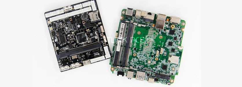
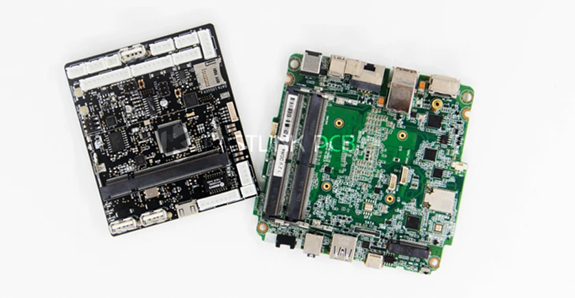
First, the tech cleans the PCB surface—dust, flux residue, whatever’s in the way. Then they shoot high-res photos of both sides. Those photos aren’t just for the file folder. They’re the reference point for forward engineering later, especially when it’s time to confirm component placement.
Remove Components (Non-Destructive vs. Destructive)
To see the traces under parts, parts usually have to come off. How they come off depends on what the team is trying to protect.
Non-destructive removal: careful desoldering keeps the original components usable.
Destructive removal: grinding is used to expose internal routing layer by layer—most often on complex boards (four layers and up).
Capture Images and Scan at 1:1
With the bare board ready, it goes onto an industrial high-res scanner. The goal is a true 1:1 image of the copper routing. On multilayer PCBs, the team repeats this step for each conductive layer. Miss a layer, and the reconstruction is going to be guesswork.
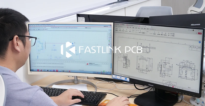
Rebuild the Layout in CAD and Pull the Netlist
Next, the scans get pulled into Altium, Eagle, KiCad—whatever the team uses. The images act as the underlay, and the engineer traces everything back in, line by line, until the digital layout matches the physical board. Then the CAD tool generates the netlist, spelling out the real connectivity between components.
Draw the Schematic
Once the layout is back, the engineer captures the schematic. That’s the “design truth” of the board. It shows how power and signals move through the circuit in a way that actually makes sense to humans. Think about it—layouts are great for manufacturing, but schematics are what engineers use to understand what the circuit is doing.
The Hard Parts of PCB Reverse Engineering
After the layers get imaged, the toughest problem isn’t “having pictures.” It’s turning those scattered images into engineering data someone can actually build from—netlist, BOM, schematic, and clean copper artwork across every layer.
High-Precision Graphic Data
Reconstructing manufacturing formats like Gerber RS274x, IPC-2581, or ODB++ is demanding because everything has to line up. Copper features can’t drift relative to solder mask, paste openings, or the stencil-cut file. Think about it—if the paste layer shifts even slightly, assembly yield drops fast. And when it’s HDI, the tolerance isn’t generous. It’s often down in the micron range, which means “close enough” isn’t close.
Complex Logic of Drilling and Via Structures
Modern boards are multilayer, and the via story is complicated. The data has to distinguish plated vs. non-plated through holes, and then it gets trickier: blind vias and buried vias, defined by which layers they connect.
Here’s the bottleneck: figuring out the start layer and end layer for each blind/buried via. Why is that so painful? Because you can’t fake stack-up knowledge. Engineers need real process experience and accurate measurement tools so the hole location, diameter, plating, and layer connectivity match what’s on the physical board.
Calibration of Component Information and Pick-and-Place Data
People underestimate how much time component data takes. Pick-and-place centroids and pin maps require clean, consistent data. That often means assigning physical coordinates to thousands of pads—manually or semi-automated—then checking it again.
And if the silkscreen is worn or missing? That’s where time disappears. Identifying the exact part number, then confirming polarity and orientation, becomes detective work. Ask any engineer who’s had a diode flipped in production—nobody wants that surprise.
FastlinkPCB’s PCB Reverse Engineering Capabilities
FastlinkPCB runs PCB Reverse Engineering like an engineering project, not a guessing game.Complex custom parts? Covered. Designs that touch programming logic and IP? The team has a proven path for that as well. And when a board depends on discontinued components, FastlinkPCB can usually replace them cleanly by combining sourcing channels with technical verification—so the replacement behaves the way the original part did.
It doesn’t stop at reconstruction, either. FastlinkPCB can carry the job through PCB manufacturing and PCB assembly, which keeps handoffs simple and timelines tighter.Have questions about PCB Reverse Engineering, or worried about a specific board? Reach out and talk it through.