
- On July 23, 2026
- In blog
PCB vs. PCBA: A Manufacturer’s Guide to the Differences
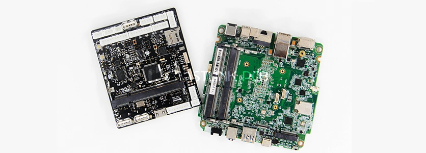
If you have ever opened up a smartphone or a laptop, you have likely seen the flat, green board covered in silver chips and copper traces. In everyday conversation, most people simply call this a PCB (Printed Circuit Board). However, from a professional electronics manufacturing perspective, that label is only half accurate.
When the board is completely bare, it is a PCB. But once it goes through the assembly line and is densely populated with integrated circuits (ICs), resistors, and other electronic components, its identity upgrades to a PCBA (Printed Circuit Board Assembly).
As a full-turnkey PCB fabrication and assembly partner, FastlinkPCB is here to break down the core distinctions between these two terms. In this guide, we will dive into their fundamental structures and map out exactly how they differ in design, manufacturing workflows, real-world applications, and production costs.
1.What is a PCB?
PCB is a flat, rigid or flexible plate made from insulating material that serves as the baseline structural foundation for virtually all modern electronics. In its bare-board state, a PCB contains absolutely zero electronic components and possesses no active functionality or processing power. Its sole purpose is to provide the physical, mechanical skeleton to support components and the internal electrical network to route signals between them.
Core Structure and Materials
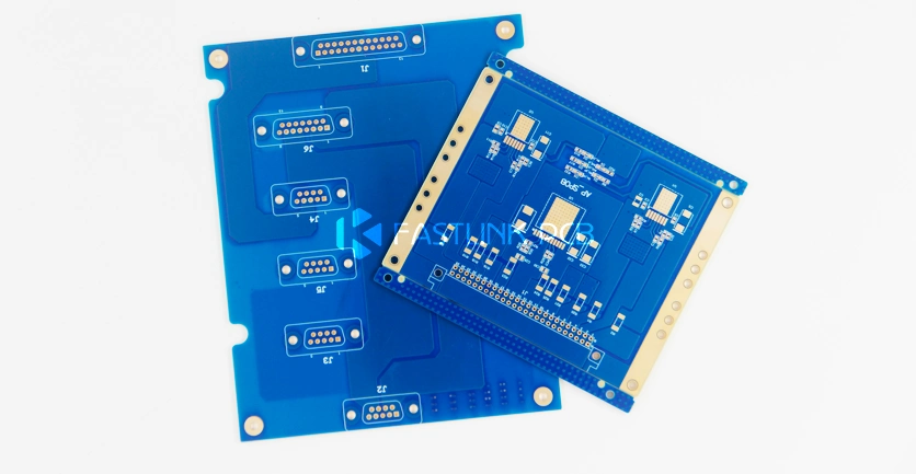
A modern PCB is a composite matrix built from several layered materials, each fulfilling a specific mechanical or electrical role:
- The Substrate (Dielectric Layer): This functions as the non-conductive core skeleton of the board. The overwhelming industry standard is FR-4, a flame-retardant woven fiberglass cloth bound with an epoxy resin. However, advanced designs may swap FR-4 for flexible polyimide films, aluminum cores (for heat dissipation), ceramics, or high-frequency PTFE (Teflon) matrixes.
- Copper Foils and Signal Traces: Sheets of ultra-thin copper foil are laminated directly onto the substrate. Through a selective chemical etching process, excess copper is stripped away, leaving behind a network of fine tracks, planes, and pads. These traces act as the physical wiring that channels electricity and data signals between components.
- Vias (Vertical Interconnect Access): Vias are miniature conductive barrels drilled through the board. Plated with copper, they bridge signals between different copper layers. They can pass completely through the board (Through-Hole Vias), connect an outer layer to an inner layer (Blind Vias), or link internal layers entirely hidden from the surface (Buried Vias).
- Solder Mask: This is a protective, liquid polymer coating applied over the outer copper layers. Most famously green—though available in black, blue, red, and white—its job is to insulate the bare copper traces, prevent accidental short circuits, and isolate the exposed pads so that solder only adheres where intended.
- Silkscreen: This is the top layer of printed ink (typically white) stamped onto the board. It features human-readable text, component outlines, polarity markers, and reference designators (like R1, C1, U1). This text acts as a map for automated assembly machinery and technicians during population, testing, and field troubleshooting.
Applications
From consumer hardware like smartphones, laptops, televisions, and home appliances, to industrial machinery, automotive ECUs, medical imaging systems, and aerospace avionics—virtually any hardware that relies on multiple electronic parts requires a PCB.
However, it is worth noting that a bare board is entirely passive. It only transitions from a structural placeholder into an active, functional circuit once it completes the assembly process, where active chips and passive components are permanently bonded to its pads.
2.What is a PCBA?
Simply put, a PCBA is a fully functional, finished electronic circuit module. Unlike a blank, unpopulated bare PCB, a PCBA comes loaded with all the active and passive silicon elements required by the schematic design. Once powered, it is fully capable of running firmware, processing signals, and executing system commands.
In factory vocabulary, “PCBA” also acts as a verb, referring to the entire technical ecosystem of populating and reflow-soldering those components onto the underlying board.
To bring a bare board to life, contract manufacturers rely on two primary assembly methods, often mixing both on a single project:
Surface Mount Technology (SMT)
SMT is a high-speed, heavily automated, and flexible manufacturing method that mounts components directly onto the outer copper pads of the PCB. By eliminating the need to pass component leads through drilled holes, SMT accommodates ultra-tight pin pitches and massive component densities, enabling engineers to cram massive processing power into miniaturized enclosures.
The standard automated SMT staging sequence involves:
- Solder Paste Deposition: Stencil printers screen a microscopic layer of viscous paste onto the open landing pads.
- Component Pick and Place: High-speed chip shooters pick components from continuous tape reels and place them onto the paste with micron-level alignment.
- Reflow Soldering: The populated assembly travels through a multi-zone reflow oven, heating the paste into a liquid alloy before cooling it into solid, shiny metallic joints.
- In-Line Quality Inspection: Boards run through automatic visual audits (SPI and AOI) at strategic steps to intercept printing alignment shifts or component placement offsets prior to final packaging.
Through-Hole Technology (THT)
THT is a more traditional manufacturing workflow where component leads are inserted through pre-drilled holes in the PCB and soldered from the opposite side. While older than SMT, THT remains vital in modern manufacturing because it provides excellent mechanical bonding strength. This makes it the go-to choice for heavy, bulky, or high-stress parts that must withstand harsh environments or constant physical strain.
Whether executed via automated insertion machinery or manual hand-assembly stations, the THT sequence follows these steps:
- Precision Drilling: During the bare-board phase, holes are drilled through the substrate matching the exact lead pitch and diameter of the component.
- Component Insertion: Technicians or radial/axial insertion machines guide the component leads down through the plated through-holes.
- Wave Soldering: The underside of the board passes over a continuous wave of molten solder. The liquid alloy wicks up into the plated barrels via capillary action, locking the pins into a robust metallurgical joint.
- Post-Assembly Verification: The completed assembly undergoes electrical bench testing and visual checks to ensure zero cold joints, voids, or short circuits.
3.How PCB and PCBA Fit Together
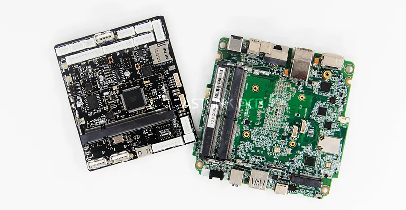
Ultimately, a PCB and a PCBA are the exact same product viewed at two different points along the manufacturing timeline. The core distinctions and operational ties between them boil down to a few key areas:
- Functional Transformation: A bare PCB is a passive blueprint—an empty matrix with no processing power or electrical capability. A PCBA is a complete, active circuit network. It is the plug-and-play engine ready to be installed into an enclosure and powered up right out of the box.
- Manufacturing Complexity: Fabricating a raw PCB is a localized, linear material process involving etching and lamination. Building a PCBA is a massive logistical and technical undertaking. It requires sourcing and tracking thousands of distinct line items from a global component supply chain, managing strict moisture-sensitivity levels (MSL), and cross-coordinating high-speed SMT, manual THT, and multi-zone reflow profiling.
- Cost Structure: The financial profiles of the two are completely different. A bare PCB represents a relatively small fraction of your total build cost, calculated primarily on board size and layer count. A PCBA’s price tag scales significantly because it absorbs the raw material costs of active silicon, microcontrollers, and connectors, alongside automated programming overhead, specialized assembly labor, and strict yield-testing routines.
- Absolute Interdependence: You cannot have one without the other. A PCB serves as the foundational architecture; a PCBA is the realization of that architecture. PCB fabrication is the mandatory phase-one baseline, and PCBA assembly is the downstream phase-two completion.
- Packaging and Logistics Standards: Because their structural properties shift dramatically during assembly, their handling profiles must shift too. A stack of bare PCBs is chemically stable and robust, requiring only simple plastic vacuum-sealing to prevent moisture ingress.
In contrast, a finished PCBA is populated with highly sensitive integrated circuits vulnerable to physical impact and electrostatic discharge (ESD). Consequently, factories ship completed PCBAs wrapped in heavy-duty ESD-shielding bags, anti-static bubble wrap, and specialized partitioned trays to eliminate the risk of a field failure before the product even arrives.
4.PCB vs. PCBA: Manufacturing Dynamics & Cost Structures
When mapping out an electronics hardware product, understanding how cost drivers, fabrication complexities, and scaling mechanics diverge between a bare board and a populated assembly is critical for budget accuracy. A raw PCB is merely a structural baseline, whereas a PCBA is a unified, intelligent system. Consequently, their financial profiles and engineering hurdles sit on completely different levels.
Bare PCB
The manufacturing difficulty and baseline cost of a bare board are dictated entirely by its physical stackup, trace geometry, and raw material selection.
- Cost Drivers: Raw PCB pricing is tied directly to physical dimensions, layer counts, routing density (such as ultra-fine trace widths and air gaps), substrate performance (standard FR-4 vs. specialized high-frequency RF laminates), and total volume. A basic 2-layer FR-4 board is highly cost-effective, particularly when scaled. However, moving up to a 4- or 6-layer architecture injects significant cost due to the sequential lamination cycles and extra prepreg/foil layers required.
Furthermore, adding high-density interconnect (HDI) features like blind or buried vias, locking in controlled impedance tolerances, specifying high-Tg (glass transition temperature) materials, or utilizing flexible polyimide substrates will steeply increase the per-board fabrication price.
- Primary Fabrication Challenges: On the factory floor, engineering teams must maintain tight process controls to prevent layer-to-layer misregistration in high-layer count boards, ensure drill accuracy on dense pad pitches, and eliminate material delamination (layer separation) or copper over-etching during chemical processing.
- Scaling and Turnaround: Because bare-board fabrication relies on highly linear, automated chemistry and mechanical workflows, lead times are short. Proto runs can routinely ship in just a few days. For volume production, factories optimize material utilization and slash piece-part costs through panelization—grouping multiple individual boards onto a single large manufacturing array to maximize processing efficiency.
PCBA Assembly
PCBA costs scale dramatically because they stack active component procurement, specialized labor, high-speed machine runtime, soldering consumables, and multi-stage testing on top of the bare board price.
- Bill of Materials (BOM) Costs: The BOM is almost always the single largest cost contributor of a PCBA. While passive surface-mount resistors and capacitors cost fractions of a cent, specialized Microcontrollers (MCUs), System-on-Chips (SoCs), FPGAs, or high-density connectors can easily run from several dollars to hundreds of dollars per chip. Furthermore, global supply chain bottlenecks or long lead times on critical semiconductors can inflate procurement budgets and stretch delivery timelines.
- NRE and Line Setup Fees: Prior to firing up an automated SMT line, contract manufacturers must create custom stencil tooling, calibrate feeder arrays, and program the pick-and-place vision engines. These initial engineering charges (NRE) generate a flat setup fee—typically a few hundred dollars per job.
- Low-Volume vs. High-Volume Scaling Mechanics:
- Prototypes & Low-Volume Runs: Because line setup fees and stencil costs cannot be amortized across a small number of units, prototype and short-run PCBA unit prices appear disproportionately high.
- Mass Production: As production scales into thousands of units, fixed engineering setup costs are diluted down to near-zero per board, driving unit costs down sharply. While manual hand-soldering might bypass setup fees for basic breadboards, it is far too slow, error-prone, and imprecise to handle modern fine-pitch ICs or surface-mount packages (like BGAs).
- Yield Rates & Rework Overhead: In high-density PCBA runs, achieving a 100% First-Pass Yield (FPY) across thousands of fine-pitch solder joints is challenging. Reworking misaligned chips or replacing defective components requires skilled bench technicians and specialized hot-air stations. EMS providers account for potential scrap and rework margins directly in their turn-key assembly quotes.
- Quality Assurance & Custom Functional Test Fixtures: For mission-critical electronics (such as automotive, aerospace, or medical devices), basic visual inspection is not enough. Assemblies must pass In-Circuit Testing (ICT) or Functional Testing (FCT). Machining custom “bed-of-nails” test fixtures and authoring test scripts demands upfront capital, but it serves as the ultimate firewall against field failures.
- Lead-Time Realities: Bare board fabrication typically takes between 3 to 7 business days. A full turn-key PCBA, however, requires a multi-week lead-time window. This delay is rarely caused by line runtime; rather, the factory must wait for all line-item components on the BOM to arrive at the facility from global distributors before setting up the SMT line.
Final Thoughts
At the end of the day, the real-world performance, longevity, and thermal stability of your hardware boil down to the engineering rigor of your manufacturing partner. When evaluating potential Electronics Manufacturing Services (EMS) suppliers, looking strictly at the lowest unit price is a dangerous strategy.
A truly reliable factory brings mature production engineering, international quality accreditations (such as ISO 9001, ISO 13485, and UL safety certifications), a resilient supply chain network, and end-to-end process integration under one roof. Unifying these stages minimizes handoff errors and communication gaps between the board fabricator and the SMT assembly team.
Because of these complex operational demands, full turnkey one-stop manufacturing—combining bare board fabrication, component sourcing, and PCBA assembly—has become the gold standard for modern hardware teams looking to scale fast without taking on unneeded risk.
FastlinkPCB: Your Turnkey PCB & PCBA Partner
As an industry-leading Electronic Manufacturing Services (EMS) partner, FastlinkPCB provides a seamless, end-to-end turnkey solution designed to bring your hardware concepts to market faster.
From the moment you upload your Gerber and BOM files to the final shipment of your packaged assemblies, we handle the entire lifecycle:
- High-precision bare-board fabrication
- Quick-turn prototyping
- Global component procurement and supply chain management
- Automated SMT and THT assembly
- Comprehensive QA testing (AOI, AXI, ICT, and FCT)
By keeping fabrication, procurement, assembly, and testing inside a unified closed-loop workflow, FastlinkPCB ensures your designs are built cleanly, on schedule, and to the highest industry reliability standards.