
- On September 3, 2026
- In blog
PTEF PCB Manufacturing
Substrate material selection defines the ultimate electrical performance limits of any hardware platform. When engineering applications demand low signal attenuation at high frequencies—such as RF communications, 77 GHz millimeter-wave radar modules, or 5G base station transceivers—PTFE) emerges as the premier substrate choice.
Written from a manufacturer’s perspective, this guide provides a deep technical breakdown of the core material differences between PTFE and standard FR-4 laminates, outlines the end-to-end PTFE PCB fabrication workflow, and highlights key shop-floor processing challenges along with their proven engineering solutions.
Performance Comparison: PTFE vs. FR-4 Substrates
Compared to standard FR-4, PTFE laminates deliver superior electrical, thermal, and environmental stability—making them the industry standard for high-frequency, high-reliability designs. While raw material and fabrication costs are higher, PTFE’s performance metrics fully justify its implementation in mission-critical hardware. The primary differences between the two substrates span three core dimensions:
1.Electrical Performance
PTFE Substrates: Featuring an ultra-low dielectric constant and a minimal dissipation factor, PTFE suppresses signal phase distortion and insertion loss across Sub-6GHz and mm Wave bands. This low signal delay and minimal attenuation are critical for maintaining signal integrity in high-frequency RF systems.
FR-4: The glass-reinforced epoxy matrix yields significantly higher Dk and Df metrics. This introduces severe dielectric absorption, insertion loss, and phase delay during transmission, making standard FR-4 unsuitable for high-frequency RF or ultra-speed digital circuit architectures.
2.Thermal Stability
PTFE Substrates: PTFE exhibits exceptional thermal stability, enduring continuous operating temperatures up to 260°C without mechanical degradation, structural expansion, or dielectric drift. It is engineered for high-thermal-stress applications such as RF power amplifiers, aerospace platforms, and defense electronics.
FR-4: Standard FR-4 thermal thresholds limit continuous operation to approximately 140°C. Exceeding these temperatures causes severe material degradation, matrix breakdown, and delamination, strictly limiting FR-4 usage in extreme thermal environments.
3.Environmental Resistance
PTFE Substrates: Hydrophobic properties yield a moisture absorption rate below 0.01%. Virtually zero water uptake ensures consistent electrical performance and mechanical dimensions in high-humidity environments, preventing swelling, substrate warping, or dielectric constant instability.
FR-4: Hygroscopic epoxy resin absorbs atmospheric moisture readily under humid conditions. Water absorption causes dimensional instability, alters the localized dielectric constant, and reduces insulation resistance, gradually degrading long-term hardware reliability.
4 Primary Fabrication Challenges in PTFE PCB
While PTFE delivers clear electrical performance advantages in high-frequency systems, its unique physical properties present significant fabrication hurdles. Resolving these four challenges is critical to securing high yield rates and long-term reliability in high-frequency PTFE circuit boards:
1.Material Softness, Dimensional Instability, and Placement Misalignment
PTFE laminates are inherently soft, flexible, and ductile. During mechanical drilling and routing, tool cutting forces induce localized material deformation and stress elongation. This mechanical yield causes drilled hole offsets and trace width deviations from original Gerber netlists, resulting in SMT pad misalignment during automated placement. Standard feeds and speeds engineered for rigid FR-4 will quickly compromise dimensional tolerances and lead to mass substrate scrapping on PTFE production lines.
2.Low Ablation Efficiency in Laser Microvia Drilling
PTFE dielectrics exhibit high optical transparency to ultraviolet laser wavelengths. Because UV energy passes directly through the substrate rather than absorbing as thermal energy, material vaporization fails to occur efficiently. To overcome this absorption barrier, fabricators deploy infrared CO₂ laser systems. The longer wavelength of CO₂ lasers is effectively absorbed by the PTFE matrix, cleanly ablating microvias with diameters down to 50–70 µm for blind via stackups.
3.Poor Solder Mask Adhesion to Inert PTFE Substrates
PTFE features exceptionally low surface energy and high chemical inertness, making interfacial bonding extremely difficult. While this inert behavior underpins its low dielectric loss, it prevents liquid photoimageable solder masks from forming strong chemical bonds with the raw substrate. Furthermore, PTFE’s high Coefficient of Thermal Expansion creates thermal-mechanical shear stress during reflow, increasing the risk of solder mask blistering, micro-flaking, and delamination. Fabricators mitigate this by executing plasma activation prior to solder mask coating—etching the fluoropolymer surface to increase mechanical roughness and introduce reactive chemical functional groups.
4.High Substrate & Tooling Costs
Raw PTFE laminates cost several times more than standard FR-4 materials. Beyond raw material pricing, PTFE processing demands specialized shop-floor capital investment—including CO₂ laser drills, vacuum plasma etching systems, specialized handling fixtures, extended processing cycle times, and rigorous IPC Class 3 inspection protocols. These factors combine to elevate overall fabrication costs, making PTFE substrates optimal for high-performance, mission-critical applications where signal integrity overrides strict unit cost constraints.
PTFE PCB Manufacturing Process
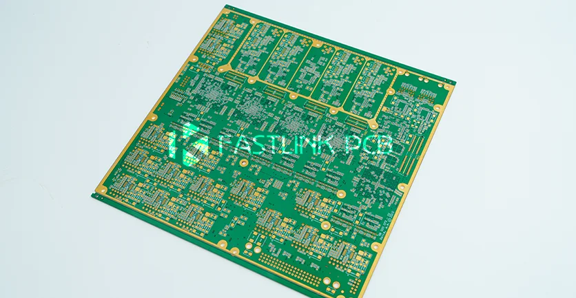
To overcome the specific physical and chemical hurdles of fluoropolymer dielectrics, FastlinkPCB executes a specialized, multi-stage manufacturing workflow. Engineered specifically around the material properties of PTFE, this process covers four critical fabrication phases from surface preparation through final inspection and shipment:
Step 1: Plasma Etching & Surface Activation
Because un-treated PTFE exhibits ultra-low surface energy, direct copper plating and solder mask adhesion fail without prior surface modification. FastlinkPCB processes panels in a low-pressure RF vacuum chamber using optimized process gases excited into a plasma state. This high-energy plasma etches the PTFE fluoropolymer surface at a microscopic level, creating a uniform, micro-rough topography with active anchor structures. This process enables mechanical interlocking and chemical bonding for subsequent electroless copper deposition and direct metallization.
Step 2: High-Precision Laser & Mechanical Drilling
The ductile, low-modulus nature of PTFE makes it susceptible to mechanical hole-wall smearing, burr formation, and fibrous strand generation under conventional drilling parameters. FastlinkPCB prioritizes non-contact laser ablation to vaporize microvias cleanly without transferring mechanical stress to the surrounding dielectric matrix. When mechanical drilling is required for through-holes, fabricators deploy specialized micro-drills featuring polished flutes, reduced spindle speeds, and optimized chip-load feed rates to prevent frictional heat buildup and hole-wall deformation.
Step 3: Controlled High-Temperature Lamination
Bonding multi-layer PTFE cores with high-profile or low-profile copper foils demands dedicated high-temperature presses capable of precise thermal-hydraulic control. FastlinkPCB utilizes programmed vacuum lamination cycles featuring ramped heating rates, controlled dwell pressures, and gradual cooling profiles. This precise thermal management relaxes internal Z-axis shear stresses induced by CTE mismatches, preventing post-lamination delamination, warp, and bow.
Step 4: High-Reliability Surface Finishing (ENIG)
Following outer-layer photolithography and pattern etching, exposed copper geometries require surface finishes that preserve trace geometry while resisting oxidation. For high-frequency PTFE PCB, FastlinkPCB extensively applies ENIG. The ENIG finish delivers a flat, co-planar surface topology, low contact resistance, high oxidation resistance, and extended shelf-life solderability—ensuring optimal signal integrity for high frequency transmission line interconnections.
Final Thought
Deciding whether to specify PTFE laminates ultimately comes down to your project’s strict performance and signal integrity requirements. Translating the theoretical high-frequency advantages of PTFE into a yields-optimized, high-reliability commercial product requires specialized fabrication expertise. Partnering with an experienced PTFE PCB manufacturer early in the layout phase is the most effective strategy to streamline prototyping and accelerate time-to-market.
If you are planning an upcoming hardware PTFE PCB design, contact the FastlinkPCB engineering team today. From dielectric material selection to complete DFM stackup evaluations, FastlinkPCB provides comprehensive technical support to ensure your product’s success from initial design through volume production.