- On July 11, 2025
- In blog
Surface Mount Technology: Advantages and Disadvantages
Since the 1960s, Surface Mount Technology (SMT) has slowly become the go-to for putting together electronic parts. It’s brought a lot of changes to how we make electronic products, especially when it comes to making things more efficient, cheaper, and smaller. Surface mount technology has its pros and cons. In this section, we’ll go over the pros and cons of surface mount technology to help you get a handle on the tech.
The Surface Mount Technology Process
Before we dive into the pros and cons of surface mount technology, let’s go over the whole process. We can only understand the technology and its role in the production process if we understand surface mount technology meaning and each step and the limits of the technology. We’ll go through this process step by step according to the standard surface mount technology process steps below.
1.Solder Paste Printing
The first step in surface mount technology assembly is solder paste printing, which involves accurately applying the appropriate amount of solder paste to the designated pad locations on the circuit board. The quality of the printing process depends on three key factors: the condition of the solder paste itself, the angle of the squeegee, and the printing speed.
If you don’t store or use the solder paste properly, even the best mounting results later on can’t guarantee product quality. For the most part, solder paste needs to be stored in a fridge. You should let it sit at room temperature for a bit before using it, and use it within two hours of opening it. Along with the quality of the solder paste, the settings on the surface mounting technology equipment need to be spot on, especially the angle and speed of the squeegee. These directly impact whether the solder paste is spread evenly and is enough.
2.Solder Paste Inspection (SPI)
Once you’ve done the solder paste printing, you can use SPI to take a look. It’s not required, but FastlinkPCB likes to do this to catch printing problems early on, avoid soldering defects down the line, and cut costs from rework. SPI is usually found in two forms: 2D and 3D. It can detect solder paste thickness, area, and offset, which helps improve overall yield rates.
3.SMD Mounting
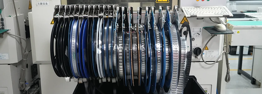
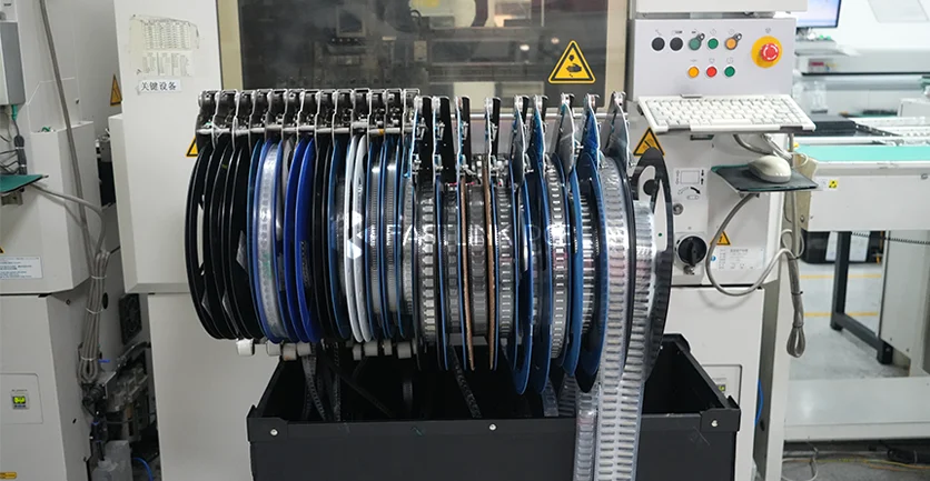
Then, it’s time to mount the components, which is done by a pick-and-place machine. There are different types of pick-and-place machines that can handle components of different sizes and precision requirements. For example, small components are usually handled by high-speed pick-and-place machines, while larger or high-precision components (like ICs, BGAs, and connectors) are processed by multi-functional pick-and-place machines. These parts often need to be lined up before you can mount them, which slows things down.
4.Visual Inspection and Manual Placement
Once everything’s in place, we’ll do a manual check to make sure everything’s lined up right and there are no missing parts. But once you start soldering, it can get tricky. Some special components, like larger DIP devices or parts that machines can’t handle, are also put in by hand at this stage.
5.Reflow Soldering
This is a key step in making sure the parts are firmly attached to the circuit board. Heating the solder paste makes it melt, which creates a strong bond between the component leads and the pads. Common lead-free solder pastes (like SAC305) have a melting point of around 217°C, so the reflow soldering temperature has to be high enough to get the job done, but not so high that it’ll damage the components. The typical reflow soldering process has a few stages: preheating, temperature rise, soldering, and cooling. The temperature curve settings have a direct impact on the soldering results.
6.Automated Optical Inspection(AOI)
After soldering is finished, we do a full inspection using AOI. This machine checks the whole circuit board for problems like missing parts, misalignment, wrong orientation, bridging, towering, edge opening, and empty solder. This stops products that don’t meet standards from moving on to the next step.
7.X-Ray Inspection (AXI)
For certain issues that are hard to spot with the naked eye or AOI, like solder joint quality beneath BGA packaging, X-ray inspection can be used. This step isn’t required for all products, but for projects that demand top-notch quality, X-ray inspection is a great extra inspection method.
8.Electrical Testing (ICT) and Functional Testing
The last testing phase is mostly about ICT and functional testing. ICT is used to check for basic circuit problems, like open circuits or short circuits. It usually verifies that components like resistors, capacitors, and inductors on the board are working. Functional testing simulates the product’s actual operating conditions to ensure the entire board functions as intended. When you combine these tests, they make the final product way more stable and reliable.
Advantages of Surface Mount Technology
1.Miniaturized Design
Surface mount technology components are a lot smaller and take up less space than traditional through-hole components. In fact, they can reduce space requirements by 60% on average, and in some cases, up to 90%.
2.Improved High-Frequency Performance
Surface mount technology components don’t have long leads or only short ones, which reduces the circuit’s distributed parameters and minimizes radio frequency interference. So, SMT circuit boards work better at high frequencies.
3.High-Speed Signal Transmission
Surface mount technology-assembled components also have a high density. With double-sided PCBs, you can get up to 5.5 to 20 solder joints per square centimeter. Since there are hardly any short circuits or signal delays, surface mount technology-assembled circuit boards can handle high-speed signal transmission, making them perfect for high-speed electronic devices.
4.Simplified Production Process
In the surface mount technology process, component leads don’t need to be bent, formed, or trimmed, which makes the whole assembly process more streamlined and efficient. surface mount technology is way faster than traditional through-hole mounting technology. It can reduce total production costs by 30% to 50%.
5.Advantages of Automated Production
Automation is key in surface mount technology. It makes the process more efficient and consistent. This helps reduce component failures caused by the soldering process.
6.Reduced Material Costs
Another perk of automated production is that it uses less packaging materials, which brings down the manufacturing costs. Most surface mount technology components are cheaper to package than similar through-hole components. This makes surface mount technology components more cost-effective than traditional components and helps us save money.
Disadvantages of Surface Mount Technology
1.High Equipment Costs
A lot of surface mount technology devices, like reflow ovens, pick-and-place machines, solder paste screen printers, and hot air rework stations, usually require a big investment. Since they’re so expensive, setting up a full surface mount technology production line is a big investment for any business.
2.Difficult Inspection
Since a lot of surface mount technology components have small size and many solder joints, inspecting them is more challenging. For instance, BGA-packaged components usually have solder balls under the component, which makes it hard to inspect the solder joints. The required surface mount technology inspection equipment is also pricey, which adds to the operational burden for many companies.
3.Susceptibility to Damage
SMD parts are usually very precise, but they can get damaged during shipping or putting together. They’re also highly sensitive to static electricity, so you’ve got to be careful when you handle and package them. You need a cleanroom environment during production to make sure the components are up to snuff.
4.Power Limitations
Not all active and passive components are suitable for SMD use. Most SMD components have lower power ratings, so surface mount technology isn’t suitable for applications requiring high power.
Final Thoughts
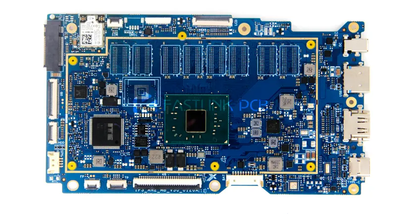
FastlinkPCB offers professional PCB assembly and manufacturing services. We’ve been doing this for 16 years, with experience in surface mount technology and through-hole assembly. Our production process is mostly automated, with most of the component placement happening automatically. When we need to, we also do manual operations to make sure every detail is exact and there are no mistakes. We can deliver on time and within your budget, whether it’s a prototype or a large production run.
If you’d like to know more about integrating high-quality SMT technology into your PCB components, just give us a shout.