- On January 22, 2026
- In blog
The Complete Guide to Gold Finger PCB Manufacturing: Standards, Plating, and Design
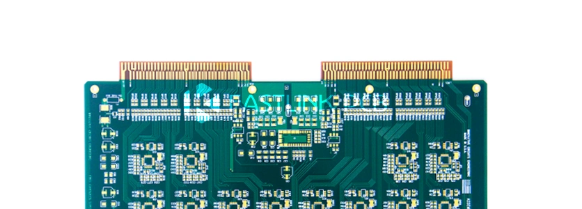
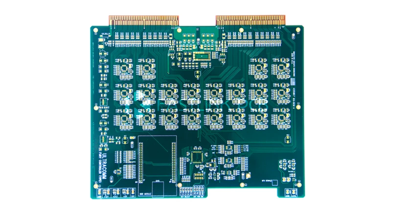
When you slide a high-performance GPU into a server or swap out communication cards in an industrial rack, every bit of current and high-speed data squeezes through those narrow gold contacts known as gold finger pcb. These gold stripes aren’t just there for aesthetics; they are the most heavily stressed part of the PCB. They have to withstand constant friction and repeated plug-in cycles while maintaining perfect conductivity without any oxidation or flaking. This guide provides a deep look at the plating process, essential design rules, and the manufacturing hurdles involved in gold finger pcb production.
What is Gold Finger PCB?
“Gold Fingers” might sound like a catchy nickname, but it’s a vital technical term for the row of gold-plated contacts lined up along the edge of your PCB. Why “fingers”? Simply because they are long, narrow, and arranged just like… well, fingers.
Think of them as the “golden bridge” between your board and the rest of the machine. If you’ve ever looked at a graphics card, a sound card, or a network card, you’ve seen them in action. They are the primary interface for PCIe and PCI slots. When you slide that card into the motherboard, these fingers make a tight, high-pressure connection to handle the heavy lifting: power delivery, data transfer, and signal talk.
We use gold here for a very specific reason. Because these contacts have to deal with the friction of being plugged in and the risk of oxidation, gold is the only material that gets the job done reliably over time. Without this bridge, your high-performance hardware wouldn’t have a way to talk to the rest of the system.
The Gold Finger PCB Plating Process(ENIG vs Hard gold)
When it comes to gold fingers pcb, we see two very different plating methods. Understanding the difference is the only way to make sure your board doesn’t fail in the field.
1.Electroless Nickel Immersion Gold (ENIG)
We use ENIG all the time for regular surface pads. It’s flat, it’s easy to solder, and it’s cost-effective. But for gold fingers? It has a massive weak spot. The gold layer is only 2 to 5 micro-inches thick, and it’s “soft.” Think about it: every time you slide that card into a slot, you’re scraping that thin layer. It doesn’t take long for the gold to rub off, leaving the nickel exposed to the air. Once that happens, you’ve got oxidation and a dead connection.
2.Electroplated Hard Gold
If your card is going to be plugged and unplugged more than a few times, you need hard gold. It is the gold standard for a reason.
Why? Because we don’t use pure gold here. We add a tiny bit of cobalt or nickel into the plating to make it strong—much stronger than the soft gold used in ENIG. We also plate it much thicker, usually at least 30 u”. This thick alloy layer is built to take a beating. It can handle the friction of a high-pressure connector slot day after day without flaking or wearing down. If you want a connection that stays stable and keeps the resistance low for years, this is the way to go.
Gold Finger PCB Design Specifications
1.Gold Plating Thickness Specifications
Let’s get into the heart of gold finger pcb reliability: thickness. This is where your wear life and contact quality live or die. But here is the thing—you don’t want to just throw the thickest layer of gold possible at your board. Why? Because gold is expensive, and over-engineering is just as bad as under-engineering. You need to find that zone where cost meets performance.
We follow IPC-4556 and IPC-6012 standards, sure, but those are just the floor. You need to think about how your board is actually going to be used in the real world.
Here is how we usually break it down for our clients:
- The “One and Done” (< 5 u” ENIG/ENEPIG): Think of this as a protective skin. It keeps the board from corroding and makes it easy to solder, but it hates friction. If your card is going to be plugged in once and then forgotten for five years, this works.
- The “Middle Ground” (10 to 15 u” Thin Hard Gold): It’s tougher than ENIG, but it still has a thin margin for safety. It’ll survive a few swaps, but we don’t recommend it if your hardware is critical. It’s a bit of a gamble to save a few bucks.
- The “Pro Standard” (30 to 50 u” Hard Gold): This is the heavy hitter. If you’re designing PCIe cards, memory modules, or industrial gear that sees a lot of action, this is your go-to. It’s built to take a beating and keep the resistance low.
Most of the time, that 30 to 50 u” range is exactly what you want. Concerned about the bill? We can get smart with it. We use selective plating to put that thick gold exactly where the pins hit the board, so you get the performance of a high-end card without paying for gold you don’t use.
2.Precise Solder Mask Opening
There is nothing worse than getting a board back only to find solder mask ink bleeding onto your gold fingers. To keep those contacts clean, you need to design a solid “solder bridge” between the mask and the gold. You want that contact area perfectly flat and free of debris. If the ink overflows, you’re looking at intermittent connection issues from day one.
3.Avoid Via Layout Near Edges
Here is a rule we never break: Keep your vias at least 1.0 mm away from the gold fingers. Why? Because every time you shove that card into a slot, the board flexes. That mechanical stress likes to find the weakest point, which is usually the copper inside a via. If a via is too close to the edge, it’ll crack under the pressure, and your signal is gone.
4.Design Guiding Bevels
Think of the lead-in edge of your board like a ramp. You want a 30° to 45° bevel there so the board slides into the socket like a glove. Without that chamfer, the square edge of the PCB will hit the connector pins like a hammer, wearing them down or even snapping them. It’s a tiny manufacturing step, but it’s the secret to a long-lasting board.
5.Clear Labeling of Dimensions and Processes
We see a lot of PCB designs, and the ones that succeed always have great documentation. Make sure your fabrication drawings call out the exact dimensions, the plating thickness, and the bevel requirements. Don’t assume the shop knows what you want. Clear labels are the only way to make sure the board we build is the board you actually need.
Challenges in Gold Finger PCB Manufacturing

Look, gold finger defects aren’t just bad luck. They are usually the result of a chemical reaction that went off the rails or a design that didn’t leave enough room for error. We spend a lot of time on the factory floor tracking these issues down. If you are an engineer or a buyer, you need to know what to look for so you don’t end up with a batch of dead boards.
1.Plating Delamination
If you have ever seen a gold layer peel away like an old sticker, you have seen delamination. It’s a total disaster. The second you slide that card into a slot, the gold flakes off and the connection dies.
- Why does it happen? Most of the time, the surface wasn’t cleaned properly during pre-treatment. Think of it like trying to paint a greasy wall—it’s just not going to stick. Also, if your nickel barrier is too thin (we are talking under 3 microns), it can’t do its job as a “glue” for the gold.
- How do we fix it? We don’t take chances with surface prep. We use a deep micro-etch to “wake up” the surface before any gold touches the board. Then, we use XRF (X-ray Fluorescence) tools to scan the boards and make sure that nickel layer is a solid 3 to 5 microns thick.
2.Surface Pitting
If you spot tiny pinholes or oxidation marks on your gold fingers pcb, you’re likely dealing with high porosity. It’s a common headache for boards heading into humid or high-sulfur industrial areas.
- Why does it happen? Think of your gold plating like a shield. If your hard gold is thinner than 0.5 microns, that shield becomes porous—almost like Swiss cheese. It’s not a solid wall, so corrosive elements from the air sneak through those tiny gaps and start eating away at the nickel underneath.
- How do we fix it? For any “heavy-duty” application, we don’t mess around with thin plating. We push the hard gold thickness to 0.8–1.5 microns to make it airtight. Plus, we always use moisture-proof vacuum packaging with desiccants to make sure the boards stay pristine during shipping and storage.
3.Discoloration and Nickel Diffusion
There is nothing worse than a high-end card that looks like it’s rusting. If your gold fingers pcb are losing that “bright gold” look and turning a muddy red or brown, you’ve got a diffusion issue.
- Why does it happen? Two reasons. First, the gold bath in the factory might be contaminated with copper or other gunk. Second, and more commonly, the gold layer is just too thin. Believe it or not, nickel atoms can actually “crawl” through thin gold to get to the surface. Once they hit the air, they oxidize and turn the whole finger a dark, blotchy color.
- How do we fix it? We treat our chemical baths like a science lab—keeping the pH between 4.0 and 4.5 and the heat around 50–60°C. But the real key is the thickness. We ensure at least 0.5 microns of gold to act as a “deadbolt” that keeps the nickel atoms trapped where they belong.
4.Poor Adhesion
If your plating starts showing micro-cracks after a few heat cycles or just from being handled, you’ve got an adhesion problem. It’s like trying to tape something to a glass window—if it’s too smooth, it’s not going to hold.
- Why does it happen? Either the substrate was too “shiny” and didn’t have enough texture for the metal to grab onto, or the electrical current was jumping all over the place during plating. When the current isn’t steady, the metal doesn’t settle in a tight, solid structure—it stays loose and fragile.
- How do we stop it? We make sure the surface has a bit of “teeth” by keeping the roughness (Ra value) at 0.5–1.0 microns during prep. This creates a mechanical lock. Then, we watch our current density like a hawk to make sure the metal builds up in a smooth, consistent layer.
5.Uneven Plating
Ever get a batch of boards where some gold fingers look great but others look thin and washed out? That’s uneven plating. It’s a double-edged sword: the thin ones wear out too fast, and the thick ones are brittle (and expensive!).
- Why does it happen? Usually, it’s a layout problem. If the fingers are packed too tightly in one spot or stuck out on a lonely corner of the panel, the electrical current won’t hit them evenly. It’s called the “shielding effect.” If the chemicals in the tank aren’t flowing perfectly, you’ll get “dead zones” where the gold barely plates at all.
- How do we stop it? We don’t just “hit go” on the plating machine. We carefully design the panel layout to balance the current across every single finger. For high-precision gold bonding work, we use automated, high-speed circulation systems. This keeps the gold thickness rock-steady across the entire board, so every contact performs exactly the same.
How to Test Gold Finger PCB
Let’s be real: in this business, “looking good” isn’t the same as “performing well.” You can’t tell if a gold finger is going to flake off just by staring at it. Here is the “stress test” every board goes through at our factory:
- Under the Microscope: We don’t just glance at the contacts; we get in close. Using 10x to 20x magnification, we scan every edge for micro-pits or the slightest hint of peeling.
- The X-Ray Scan (XRF): We use X-ray Fluorescence (XRF) to see through the surface. It tells us exactly how thick that gold layer is down to the micro-inch. No “thin plating” and no cutting corners—you get exactly the gold you paid for.
- The “Stay Put” Test: We follow the IPC tape test protocols to check adhesion. We apply high-strength tape and pull—if even a speck of gold comes off, the whole batch is out. Your gold needs to stay put through years of plug-in cycles, and this is how we prove it will.
- Simulating the Real World: Most boards don’t live in clean offices. They live in hot, salty, or humid industrial racks. We run salt spray and thermal cycling tests (based on MIL-STD-883) to beat these boards up in the lab. We want to see where the breaking point is so we can make sure your design stays well within the safety zone.
Choosing a Professional Gold Finger PCB Manufacturer
At the end of the day, your design is only as good as the shop that builds it. When you’re dealing with something as sensitive as gold fingers pcb , you need a partner who doesn’t just “take orders” but actually understands the physics and chemistry behind the board.
That is where we come in. At FastlinkPCB, we’ve spent years in the trenches solving the exact plating, adhesion, and thermal challenges we’ve discussed in this guide. We don’t just plate PCB; we’ve built a complete, closed-loop quality system.
Need a second pair of eyes on your stackup? Or maybe you’re worried about how your bevel angle will hold up in a specific chassis? We’re here to help. From early-stage design advice to scaling up your production, the FastlinkPCB team is ready to get to work.