
- On August 31, 2026
- In blog
Understanding Mobile PCB: Key Components, Common Issues, and High-Density Manufacturing
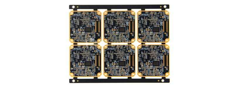
As smartphones continue to shrink in thickness while scaling up in processing power, modern hardware architectures rely heavily on ultra-compact Mobile PCBs. Serving as the central nervous system of the device, the Mobile PCB must integrate primary processors, flash storage, power management ICs, and wireless communication modules within an extremely constrained physical footprint—all while ensuring stable power delivery and low-latency signal integrity. Device performance and long-term reliability depend directly on the precision and quality of this central substrate.
Engineering a Mobile PCB presents extreme technical challenges. High-density routing, microscopic microvias, and tight component spacing leave zero margin for error; thermal buildup or mechanical drop impact can easily compromise structural integrity. Meeting these demands requires advanced HDI design and specialized fabrication techniques far exceeding standard rigid board standards.
This guide breaks down the core architecture of Mobile PCBs, common failure modes, diagnostic troubleshooting protocols, and the primary fabrication hurdles in high-density manufacturing.
Mobile PCB Layout
The ability of modern smartphones to deliver high-performance computing within an ultra-slim chassis relies on the layout integration of three primary subsystem domains:
Substrate Placement
Central Processor Scheduling: The Application Processor serves as the system compute engine, orchestrating OS execution and application workloads.
Thermal Isolation & Performance Throttling: Positioning the AP requires balancing short interconnect routes for signal strength against spatial separation from secondary heat sources. Concentrating thermal loads leads to junction overheating, triggering aggressive frequency throttling and system lag.
Thermal Optimization
Efficient Power Distribution: The Power Delivery Network routes current from the battery across dedicated PMIC rails to supply low-voltage digital cores, display panels, and peripheral ICs without excessive voltage drop.
Dynamic Power Scaling: Integrating dedicated PMIC topologies enables Dynamic Voltage Scaling, dynamically tuning voltage levels and rail currents based on real-time CPU/GPU workloads to maximize battery efficiency.
Thermal Dissipation Paths: Strategically placed thermal via arrays, copper ground pours, and integrated heat spreaders rapidly draw heat away from active silicon into the outer frame, ensuring sustained device reliability.
Signal Integrity Design
Wireless Connectivity: The RF section processes multi-band cellular, Wi-Fi, and Bluetooth signals, demanding continuous transmission paths with minimal parasitic loss.
Shielding & Crosstalk Isolation: Antenna elements and transceiver ICs are isolated using metal shielding cans, dedicated ground planes, and differential routing to suppress cross-channel EMI. Controlled impedance routing minimizes reflection and insertion loss.
High-Frequency Substrate Selection: For high-frequency 5G mmWave and Sub-6GHz bands, substrates utilize low-loss dielectric laminates like PTFE or ceramic-filled materials to minimize dielectric absorption.
Understanding these core functional zones allows hardware engineers to treat the PCB layout as a functional roadmap, enabling rapid fault isolation during power-on failures or RF link degradation.
Mobile PCB Troubleshooting
Locating and repairing hardware failures on high-density mobile PCBs requires systematic diagnostic workflows. Below is a breakdown of primary failure modes, common diagnostic traps, and failure analysis best practices:
1.Primary Hardware Failure Modes
- Short Circuits: Typically caused by solder bridging during reflow or liquid ingress inducing dendritic growth across component pads.
- Trace Fractures: Signal line disconnections resulting from mechanical drop-impact micro-cracking, board flexing, or copper trace galvanic corrosion.
- Thermal Stress: Passive components (MLCCs, resistors) and active ICs suffering dielectric breakdown or thermal burnout from transient voltage spikes.
2.Diagnostic Pitfalls and Mitigation Strategies
- Component Misidentification: Micro-passives and power management ICs often feature minimalist top-marking codes that are easy to misread under low light.
- Mitigation: Cross-reference component marking specs against an unpopulated golden board or official board schematics/bitmap files.
- Overlooking Micro-Passives: Decoupling capacitors and pull-up resistors placed adjacent to high-density BGA packages are easily knocked off or fractured during handling.
- Mitigation: Perform visual inspections under high-magnification optical microscopes, scanning package edges for solder bridges, mechanical burrs, or missing pads.
- Corroded or Obscured Laser Markings: Liquid ingress, thermal charring, or faint laser etchings obscure chip identification codes, impeding component replacement and chip-off data recovery.
- Mitigation: Utilize high-definition reference photos or perform thermal imaging and point-to-point pinout mapping against a working reference PCB.
3.Standard Inspection
- Visual & Optical Screening: Inspect board physical geometry, solder fillet integrity, component orientation, and marking codes under optical magnification.
- Rework Inspection: Examine component borders for residual flux, misaligned packages, or manual soldering burrs indicating prior repair attempts.
- 3D X-Ray Inspection: Deploy X-ray inspection systems to non-destructively evaluate internal BGA solder ball voiding, package micro-cracks, and buried microvia integrity.
- Parametric Electrical Probing: Use digital multimeters and oscilloscopes to probe designated netlist test points to confirm power-rail voltages and signal continuity.
Manufacturing Challenges of Mobile PCBs
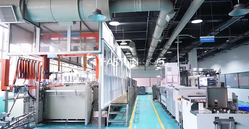
However, many faults that appear to be caused by improper use often stem from quality defects on the manufacturing end. Because the space on a mobile phone PCB is extremely compact, accurately implementing these designs on the production line itself faces huge technical challenges.
Mobile PCB Material Selection
- Standard FR-4 Materials: Possess good flame retardancy and electrical insulation properties, being cost-effective and reliable in performance, suitable for the vast majority of standard mobile phone PCBs.
- Polyimide (PI): Features excellent flexibility, heat resistance, and electrical stability, making it the first choice for creating flexible and durable foldable phones (flex boards).
- Polytetrafluoroethylene (PTFE / Teflon): Has an extremely low dielectric constant, minimizing signal loss at high frequencies; specially designed for high-frequency, RF, and 5G applications to significantly enhance signal integrity.
- Ceramic Substrates: Possess high thermal conductivity and excellent durability, suitable for high-power, high-performance components, providing efficient thermal management and extremely high reliability.
High-Density Interconnect Engineering
- Crosstalk & EMI Mitigation: In ultra-compact HDI stackups, routing high-speed digital buses parallel to sensitive RF traces introduces severe cross-coupling. Layout fabricators enforce strict 3W trace clearances, continuous ground reference planes, and laser-drilled shielding microvias to preserve signal integrity and prevent data corruption.
- Ultra-High Component Placement Density: Mounting thousands of sub-01005 passives and 0.35 mm pitch BGA packages onto micro-pads leaves zero tolerance for placement offset. Fabricators must maintain tight solder mask clearances, employ modified Semi-Additive Processes (mSAP) for sub-30 µm trace widths, and verify that every microvia-in-pad is filled and planarized to prevent solder wicking and joint failure.
Mobile PCB Assembly and Soldering Requirements
- Precision SMT:SMT pick-and-place systems position sub-01005 passives and micro-BGA packages onto high-density pad geometries with sub-micron placement accuracy. Thermal reflow profiles are tightly calibrated to establish robust intermetallic bonds while preventing thermal shock or component warping on ultra-thin substrates.
- High-Speed Interconnect Technologies:Mobile hardware architectures leverage board-to-board connectors and flexible printed circuits (FPCs) to establish multi-gigabit module interconnections. For 5G mmWave and high-speed bus architectures, low-profile, high-frequency coax-to-board connectors preserve transmission line impedance, mitigating insertion loss and signal degradation.
Multi-Stage Quality Inspection
- 3D AOI: Automated Optical Inspection screens board surfaces for component misalignment, tombstoning, solder bridging, and surface fillet flaws post-reflow.
- 3D AXI: Automated X-Ray Inspection non-destructively penetrates multi-layer HDI stackups and bottom-terminated components, isolating micro-voiding beneath BGA solder balls, buried via cracks, and insufficient barrel plating.
Selecting the Right Mobile PCB Manufacturing Partner
In mobile electronics fabrication, every layout detail directly governs overall device performance and long-term hardware stability. FastlinkPCB specializes in high-precision manufacturing for HDI stackups, micro-blind and buried vias, and ultra-high-density smartphone substrates. Backed by end-to-end 3D AOI/AXI inspection protocols and an engineering team with over 16 years of hands-on expertise, FastlinkPCB provides turnkey services—from front-end DFM analysis to volume Mobile PCB fabrication and SMT assembly.
Partner with FastlinkPCB
Ready to initiate your next mobile hardware project? Contact the FastlinkPCB engineering team today to submit your Gerber or ODB++ design files for a complimentary DFM evaluation and a fast, competitive manufacturing quote.