- On April 19, 2026
- In blog
What Is IC Substrate?
The tech gap between silicon wafer and traditional PCB is widening fast. Experts expect the advanced IC substrate market to hit $11.37 billion by 2026. This growth isn’t a fluke. Why is it happening? Because AI accelerator demand for raw power is forcing the supplier to push past physical limit—shrinking line width and spacing to under 10 micron. What was once a lab dream is now the entry requirement for mass production.
As a buyer or engineer, look at the reality: price is no longer the main leverage. In a tight market, yield, flatness, and deep co-engineering skill are the real currency.
What Is IC Substrate Material?
Think of IC substrate material as the base dielectric for chip packaging. It acts as the bridge. It links the tiny circuit inside a chip to the PCB, providing physical support, electrical connection, and a path for heat.
What Core Function Does It Serve?
Specifically, this material handles three main task:
- Mechanical Support and Protection: It holds and carries the chip. This stops damage from physical shock or stress during assembly and shipping.
- Electrical Interconnection: It creates a signal path between a tiny chip pad and the outer board. It also links the chip to component like a resistor or capacitor.
- Thermal Management: It acts as a cooling medium. It pulls high heat away from the working chip to stop performance lag or early failure.
4 Main IC Substrate Materials
Application and performance needs dictate the choice. There are four main type of IC substrate material.
1.Organic Substrate Material: The Cost-Effective Choice
Organic substrate is the go-to for consumer electronics. Why? Because it offers a great cost benefit and a mature manufacturing process.
- Polyimide (PI): This organic material handles high heat with ease. It has great dielectric property and mechanical strength. It works best for a project that needs long-term durability.
- Epoxy Resin: Known for easy processing, strong grip, and low price. Use this for cost-sensitive mass-market product.
2.Ceramic Substrate Material: High Thermal Conductivity and Strength
When a design demands high-end cooling or high-frequency performance, ceramic is the top pick.
- Alumina: This is common in high-frequency circuit because the cost stays low and the dielectric performance is solid. It provides reliable insulation and enough mechanical strength.
- Aluminum Nitride (AlN): Thermal performance is the star here. Its thermal conductivity is far higher than alumina, yet it still keeps excellent insulation. It fits power electronics and high-performance computing (HPC) well. It pulls heat away from the chip and adds years to device life.
3.BT Resin Substrate Material
BT resin (Bismaleimide-Triazine) is a high-performance composite resin made for multi-layer IC substrate. Think about it: it offers great electrical performance (low dielectric loss), stays stable under high heat, and is physically strong. These features allow for complex, high-density multi-layer wiring. It is the favorite in car electronics, comms gear, and high-end consumer tech.
4.ABF (Ajinomoto Build-up Film)
ABF is a build-up film made for advanced chip packaging. It is a must-have for HDI IC substrate.
The big technical win for ABF is its ability to form ultra-fine line and tiny micro via. This supports 3D stack packaging and System-in-Package (SiP). It offers an ideal wiring platform for a processor or memory chip that needs a high pin count and a tiny footprint. This is exactly why ABF is now a key technology driving the next generation of AI chip and HPC.
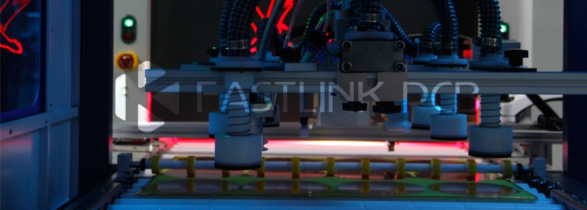
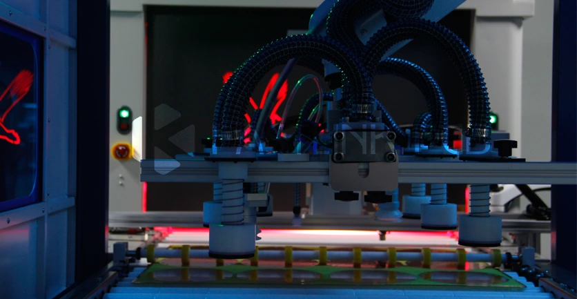
IC Substrate Manufacturing Process
Material choice dictates electrical performance and cooling, but real-world precision depends on the manufacturing tech. Today, the industry relies on three main method: Subtractive Process, Modified Semi-Additive Process (mSAP), and Semi-Additive Process (SAP). Why the evolution? Because line precision must go up as substrate size goes down.
Subtractive Process
This is the oldest, most mature way to build a PCB or IC substrate. Think of it as “removal.” A builder start with a full copper-clad substrate and etch away what isn’t needed. Usually, it use 9-12 micron copper foil. It is reliable and cheap for mass production.
But there is a catch: side etching. This limit accuracy when a line get too thin. If a design need a trace under 50 micron, yield drop. It is best for wire-bond BGA with a 35/35 micron pitch or a low-end carrier board. For a basic package where density isn’t a priority, this remains the most cost-effective pick.
Modified Semi-Additive Process (mSAP)
The logic here is different: start thin, then add. It use 1.5-2 micron ultra-thin copper. Because the base copper is so thin, etching happens fast. This stop side etching and keep the line shape square. mSAP allow for a tighter layout and a shorter signal path, which boost performance.
mSAP is the standard for BT resin substrate. It handles a 30/30 micron pitch, or even 15/15 in an advanced fab. Compared to the old way, it boost density by 2 to 4 time.
Semi-Additive Process (SAP)
SAP is the elite choice. The main difference? The base material—usually ABF film—has zero copper foil. A worker use electroless plating to deposit a tiny layer of copper on bare insulation. This creates a foundation for electroplating.
Because the start layer is so thin and even, SAP reach a level of precision that mSAP can’t touch. It handles a 15/15 micron pitch, and a shop like FastlinkPCB can even hit 12/12 micron. It cost more and need strict control, but for ultra-fine work, nothing else compare. It can build up to 12 layer for a BGA or ABF carrier board.
How to Choose an IC Substrate Manufacturer
Finding a partner to bring a design to life is often a bigger test of vision than the design itself.
1.PCB Manufacturing Precision
Think about it: if a supplier stays above a 20-micron pitch, they can’t handle an IC substrate. A top manufacturer must have the skill to push the limit below 10 micron. Anything less belongs in the past.
2.Yield Rate
In mass production, yield rate is the real currency. A reliable shop must have a testing process that is airtight. Why? Because at this level of precision, even a tiny flaw is a dealbreaker.
3.Co-Engineering Skill
A great supplier doesn’t just take a drawing and wait. FastlinkPCB gets into the work at the draft stage. The team use material knowledge to improve the design before the first board is even made. This early talk saves a team from a pricey rework later. In the advanced substrate market, competition is really about mixing expert knowledge with manufacturing detail.
The FastlinkPCB team is ready to discuss the next IC substrate project. Reach out today.