- On December 5, 2025
- In blog
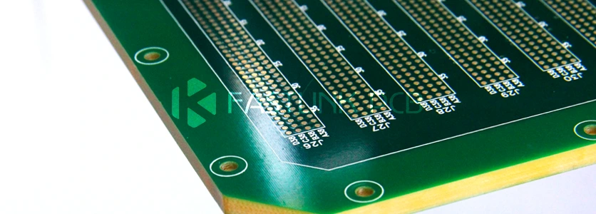
What is PCB Copper Thickness?
The current carrying capacity and reliability of a PCB are largely influenced by an often-overlooked factor: copper thickness. Whether in consumer electronics or industrial equipment built for harsh environments, each application has specific requirements for current capacity, heat dissipation, and mechanical strength. Choosing the right copper thickness is essential to meet these needs in engineering.
For designers, understanding copper thickness goes beyond just knowing the numbers in the datasheet. In PCB manufacturing, we differentiate between the base copper thickness (the initial thickness of the copper-clad laminate) and the finished copper thickness (the final thickness after processes like electroplating and etching), both of which are strictly governed by IPC standards.
What is the Standard Copper Thickness for PCBs?
In PCB manufacturing, the term “standard copper thickness” typically refers to copper foil with a thickness of 1 ounce per square foot (1 oz/ft²). This is the most commonly used and cost-effective standard, offering a good balance of cost, manufacturability, and the electrical requirements for most general applications. In terms of thickness, 1 ounce of copper is approximately 35 micrometers (μm).
However, it’s important to note that there is no universally enforced “standard” across the industry. Different PCB manufacturers may use varying “standard” copper thicknesses. Many manufacturers, for example, use 0.5-ounce copper foil for inner layers to facilitate fine-line etching. In multilayer PCB designs, manufacturers may also use different copper thicknesses for different signal or power layers, depending on the desired performance and cost balance.
For designers, the key is not to memorize a specific number, but to focus on two important points:
● Confirm the “standard starting copper thickness” for the number of layers in your design with your chosen manufacturer.
● Understand the core impact of changing copper thickness, so you can decide if a “non-standard” thickness is required.
For signal traces that carry only small currents, the electrical performance difference between 0.5 oz and 1 oz is minimal. However, for designs involving power paths, high current transmission, or temperature rise control, the difference in copper thickness becomes critical. Thicker copper reduces the DC resistance of the traces, which helps reduce voltage drop and power loss, impacting the system’s power efficiency, stability, and thermal management.
In summary, the core logic behind choosing copper thickness is: use the manufacturer’s “standard” thickness to optimize cost and lead time while meeting the requirements for current carrying, temperature rise, and impedance control. When the standard thickness does not meet the needs, specify thicker copper foil.
How to Choose PCB Copper Thickness?

1.Current Carrying Capacity and Temperature Rise
Copper thickness plays a critical role in carrying current. According to the IPC-2152 standard, the current carrying capacity is influenced by three factors: copper thickness, trace width, and the allowable temperature rise.
- Basic Relationship: With the same trace width and temperature rise, doubling the copper thickness roughly doubles the current carrying capacity. For instance, with a 10°C temperature rise, a 1oz copper and 1mm trace width can carry around 2A, whereas 2oz copper can support about 4A.
- Design Considerations: For power paths, connections to power devices (like MOSFETs), ground layers, and other high-current channels, it’s essential to use copper foil of 2oz or thicker to reduce DC resistance, lower power loss, minimize heat generation, and prevent thermal failure.
2.Trace Density and Process Capabilities
Copper thickness directly impacts the minimum trace width and spacing achievable during the etching process.
- High-Density Designs: For BGA packages, HDI, and fine-pitch signal traces, it’s recommended to use thin copper (0.5oz or 1oz). This facilitates finer and more accurate etching of traces.
- Heavy Copper Limitations: When copper thickness reaches 3oz or higher, etching efficiency decreases, and a larger minimum trace width is required. Therefore, always confirm with your manufacturer about their capability to etch thick copper to ensure your design is manufacturable.
3.High-Frequency Signal Integrity
High-frequency signals (typically in the GHz range) are mainly impacted by the skin effect, where current flows predominantly along the surface of the conductor. The higher the frequency, the shallower the skin depth. For example, at 10GHz, the skin depth of copper is only around 0.66µm.
- Strategy for Selection: For high-frequency applications (such as 5G, radar, and RF front-end designs), copper thicknesses of 0.5oz to 1oz are usually sufficient. At this point, the roughness of the copper’s surface matters more than its overall thickness. It is recommended to use RTF or VLP copper foils to reduce conductor loss.
- Copper Thickness: It is important to ensure that the copper thickness is still several times greater than the skin depth.
4.Mechanical Strength and Heat Dissipation Requirements
Copper layers are also integral to the structure and thermal management of PCBs.
- Mechanical Strength: In environments prone to vibration and shock, copper thicknesses of 2oz to 3oz can improve the PCB’s overall mechanical stability. This also strengthens the copper thickness in the through-hole walls, increasing reliability.
- Thermal Management: Thicker copper improves heat conduction. For high-power power modules, LED substrates, and motor drivers, using thick copper helps quickly spread heat from the components, reducing hotspot temperatures.
5.Cost and Manufacturing Time
- Cost Impact: Increasing copper thickness raises the raw material costs. Additionally, etching thick copper takes longer and is more challenging, which may lead to higher processing costs and yield issues. Generally, a 4oz board can be 30%-50% more expensive than a 1oz board.
- Best Practice: A mixed-layer design is a highly cost-effective approach. For instance, in multilayer boards, use 2oz or 3oz copper only for the power layers or specific signal layers that carry high current, while leaving the other signal layers with the standard 1oz copper thickness.
Final Recommendation: Collaborate Early with Your Manufacturer
Choosing copper thickness is not a standalone decision; it must be integrated with the specific manufacturing process. Before finalizing your PCB design, ensure that you communicate with the engineering team of your manufacturer to confirm that your design is within their process capabilities and to receive expert advice on optimizing your layer stack-up. This will help avoid rework and reduce project timelines.
Get in touch with the engineering team at FastlinkPCB today for a free consultation on stack-up design and quick quotes tailored to your project. Let us work together to turn your design into a reliable product.