- On November 21, 2025
- In blog
What is PCB Stencil?
While a PCB stencil does not directly conduct electricity, it plays a crucial role in ensuring components are placed accurately and efficiently, which in turn affects the overall quality and yield of the product. But how exactly does a PCB stencil work? What types of stencils are available to meet different production needs? And what should we consider when ordering a PCB stencil? In this article, we will answer all these questions in detail.
What is PCB Stencil?
In modern PCB assembly lines, the PCB stencil acts as an essential “precision template.” It is essentially a thin sheet of steel with meticulously crafted holes, and these holes align perfectly with the component pads on the circuit board.
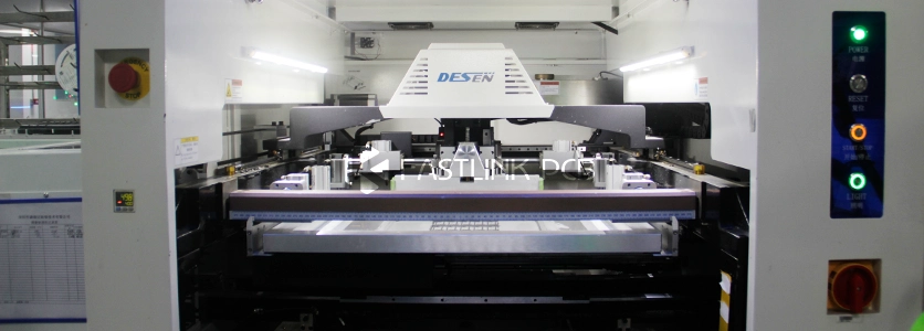
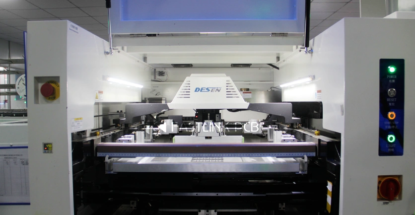
The process works like this: first, the stencil is aligned with the PCB using an optical system, ensuring they fit closely together. Then, solder paste is spread over the stencil with a squeegee. The paste flows through the holes and is precisely applied to each pad that needs to be soldered. This step is the key to high-quality SMT production, ensuring that just the right amount of solder paste is applied to each component pin. The proper amount of solder paste ensures strong, reliable solder joints.
Types of PCB Stencils

Frame-Type SMT Stencil
The frame-type SMT stencil is made from a stainless steel foil that is laser-cut with high precision and then permanently bonded and tensioned onto a durable metal frame. This design ensures excellent stability, allowing it to endure the repeated movements of the squeegee thousands of times. It is ideal for large-scale, high-speed PCB printing operations. Additionally, this stencil offers smooth inner walls and supports printing for fine-pitch components as small as 16 mils and below.
No-Frame SMT Stencil
The no-frame SMT stencil eliminates the traditional frame and consists of a separate laser-cut foil. When in use, it is fixed into place using a reusable, universal stencil fixture system. This modular approach offers two main benefits: first, it significantly reduces costs, as it is cheaper to produce, and without the bulky frame, storage and shipping costs are also lower. Second, it offers flexibility by providing seamless inner walls that support fine-pitch components below 16 mils, especially micro BGAs. This makes it a more adaptable and cost-effective solution.
Electroformed SMT Stencil
The electroformed SMT stencil is similar to the frame-type version but is permanently attached to the frame. However, the manufacturing process is quite different. It involves an additive process where nickel is plated in layers to create a single, integrated stencil made of nickel. This method results in nearly perfect, seamless tapered sidewalls, which significantly improve the efficiency of solder paste release (making it one of the stencils with the best release characteristics).
Because of this, electroformed stencils are ideal for highly challenging fine-pitch SMT applications and excel in flip-chip, wafer-level packaging, and ultra-fine-pitch μBGAs (6 to 12 mils).
What Should Be Taken into Account When Designing a PCB Stencil?
A well-designed PCB stencil can significantly improve both soldering efficiency and quality. Here are some details we should pay attention to.
Steel Sheet Thickness
The thickness of the steel sheet directly affects the amount of solder paste deposited. A sheet that is too thick can result in excess solder paste, leading to bridging, while a sheet that is too thin may cause insufficient solder paste, resulting in cold solder joints and weak solder connections.
Opening Design
The size of the stencil openings is not simply the same as the pad size. To avoid defects like solder balls and bridging, we typically design the openings to be slightly smaller than the pads. A key design rule is that the area of the PCB pad should always be larger than two-thirds of the area of the stencil opening. This helps prevent solder paste from being pulled back into the opening or migrating during the stencil release process.
Stencil Material
While high-quality stainless steel is the most common material for stencils, specialized materials like electroformed nickel perform better for ultra-fine pitch, micro BGA, or wafer-level packaging applications.
Accurate Alignment
Optical alignment marks are essential for achieving precise positioning. By placing these fiducial marks on both the PCB and stencil, our SMT equipment can achieve sub-micron alignment accuracy. This step is crucial to ensure that the solder paste is applied to the correct areas, directly impacting whether the surface-mount components are placed accurately.
Can PCB Stencils Be Reused?

Yes, a high-quality PCB stencil is designed to be a reusable tool, which plays an important role in optimizing production costs. This is largely due to the inherent durability and mechanical strength of materials like stainless steel used in stencil production. However, whether a stencil can maintain its “factory-quality” accuracy after repeated use depends on several key factors.
Stencil Quality
We use premium 301/304-grade stainless steel as the standard material, ensuring the reliability of the stencil from the very beginning.
Stencil Thickness
Stencils with a moderate thickness are generally stronger and can better endure the long-term pressure from the squeegee. Additionally, openings designed for larger pads tend to have better structural stress distribution, which contributes to a longer lifespan.
Stencil Structure
Frame-type stencils are typically more durable due to their sturdy frames, which help protect against daily collisions and friction, preventing edge damage that could affect accuracy.
Stencil Cleaning and Maintenance
Solder paste residue is the main “enemy” of stencils. To maintain their functionality, stencils must be professionally cleaned after use to remove all solder paste remnants.
Storage Environment
Dust, moisture, or extreme temperatures can damage the stencil. Storing the stencil in specialized sealed, moisture-proof bags and custom storage cabinets is the easiest and most effective way to shield it from external factors and extend its lifespan.
Wrapping Up
The PCB stencil is essential for ensuring the precision of SMT assembly. Working with an experienced manufacturing partner ensures that your stencil is perfectly aligned with your PCB design, maximizing your assembly yield. At FastlinkPCB, we are experts in this area. We offer comprehensive one-stop PCB manufacturing and assembly services. Our engineering team will provide you with the best stencil solutions tailored to your needs, along with seamless PCB assembly services. If you have any questions, don’t hesitate to contact us!