- On May 19, 2026
- In blog
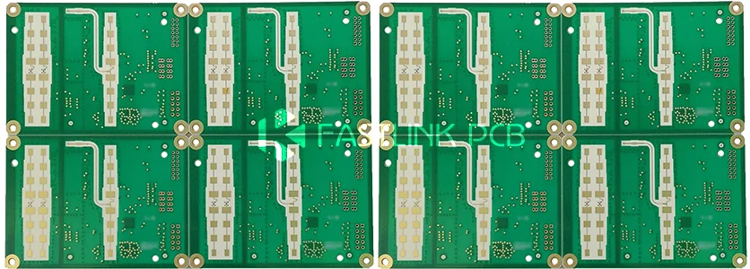
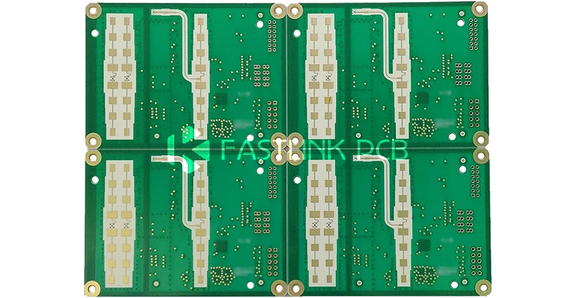
What is Radar PCB?
Think of radar as electromagnetic echolocation. It sends out a wave, catches the reflection, and clocks the round-trip time to pinpoint a target’s distance. Straightforward, right? But that operating principle puts a punishing demand on the PCB underneath. The signal runs at gigahertz frequencies. Even the slightest drift in the substrate’s dielectric constant can distort the signal and wreck the system’s detection accuracy. This article gets into radar PCB from a PCB manufacturer’s perspective.
Radar PCB vs. Standard PCB: What Sets Them Apart
Signal Frequency
A standard PCB handles signals in the kHz to MHz range — audio, video, basic digital data. A radar PCB runs in a different universe, operating across the 1–300 GHz microwave and millimeter-wave bands. At these extreme frequencies, electromagnetic waves grow hypersensitive to physical circuit geometry. A micron-scale manufacturing slip is all it takes to degrade detection accuracy or throw signal phase off course.
Manufacturing Tolerance
Standard PCB fabrication allows for a fairly relaxed tolerance window. Not so with radar. Destructive reflections along the signal path are simply unacceptable, which means impedance control has to be brutally tight. Stackup design must be dead-on precise. Advanced plating and etching processes become non-negotiable. The equipment bar and the technical bar both rise sharply for the manufacturer. Think of it this way: a standard PCB aims for “connectivity.” A radar PCB aims for “lossless replication” of the signal.
Substrate Selection
The most fundamental difference sits at the material level. Standard PCBs lean heavily on cost-friendly FR-4. But hit FR-4 with a radar signal, and its dielectric loss soaks up precious signal energy like a sponge. To preserve signal integrity, radar PCBs turn to low-loss specialty dielectrics. Get the material right, and half the radar project is already won. The question that follows: among a field of pricey specialty laminates, how does a team strike the right balance between performance demands and production cost?
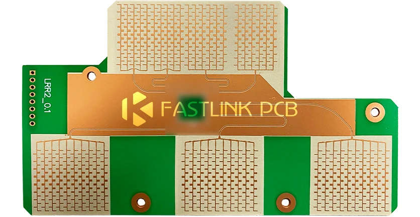
Radar PCB Materials
Substrate choice sets the ceiling for detection performance in a radar PCB. Since radar signals show zero tolerance for loss and thermal drift, manufacturers balance their options across five material categories, guided by frequency demands and the operating environment.
FR-4 and Traditional Epoxy Resin
FR-4 delivers great bang for the buck and strong mechanical properties—an electronics-industry staple. For radar, though, the shortcomings hit hard: high and unstable dielectric loss. That keeps it confined to power distribution layers or low-speed control sections. On the high-frequency RF path? FR-4 is effectively benched. Why? Because even small swings in Dk can kill signal accuracy.
PTFE (Polytetrafluoroethylene)
PTFE brings ultra-low dielectric loss (Df) and rock-steady performance over a wide frequency span. The trade-off? Picture a Teflon frying pan—slippery, soft, and a headache to machine. Mechanical rigidity is weak, processing is tough, and cost runs high. You find pure PTFE mainly in high-performance microwave front ends and precision lab gear.
Ceramic-Filled PTFE Laminate
Think of this as PTFE with a backbone. By adding ceramic filler, engineers preserve that signature low-loss character while gaining dimensional stability and mechanical muscle. It still costs more than standard materials, but it machines far more cleanly than pure PTFE. For demanding microwave radar circuits, it hits a sweet spot.
Ceramic-Filled Hydrocarbon Laminate
This material strikes a near-ideal balance: stable dielectric constant (Dk) on one side, manageable cost on the other. Thermal behavior impresses, and the price tag undercuts PTFE families by a healthy margin. The loss at very high frequencies runs a touch above premium PTFE, yet ceramic-filled hydrocarbon has become the workhorse for automotive radar modules and commercial microwave assemblies.
Metal-Backed Substrate
When a radar system pumps serious power or operates in punishing physical environments, a metal-backed substrate earns its keep. It pairs high thermal conductivity with rigid mechanical support—pulling heat out fast and keeping the board flat under stress. You will spot it in high-power weather radar, military-grade systems, and heavy industrial radar. The catch? Fabrication complexity and cost sit at the top of the curve.
Radar PCB Manufacturing Challenges
Producing a radar PCB is a different game from building a standard board. The tough spots cluster around five areas.
Substrate Processing and Lamination
Radar PCBs demand specialty materials — PTFE, Rogers laminates, and other low-loss dielectrics. Great for RF performance, a headache to fabricate. During lamination, heating rate, pressure, and cure time need control down to the second and the millimeter of mercury. One slip, and bubbles or delamination creep in. The result? Dielectric performance goes unstable.
Drilling and Etching
High-density interconnection calls for laser-drilled micro blind vias, sometimes just tens of microns across. That tiny hole makes plating uniformity non-negotiable. Anything less than “absolutely even” metallization, and you are looking at serious signal loss — or an open circuit — once frequencies climb.
Etching demands equal discipline. Tight layer-to-layer registration keeps line width and spacing rock-steady. Think of it as the heartbeat of high-speed signal integrity. Lose it, and the design falls apart.
Thermal Management
Push a radar system at high power, and the heat gets ferocious. Manufacturers embed large copper pours, thermal vias, metal backplates, even discrete heat sinks. The real trick? Bonding these dissimilar materials flawlessly without tanking electrical performance. Get that right, and the board survives under load.
Surface Treatment
High-frequency signals obsess over surface roughness. So a surface finish — ENIG, ENEPIG, silver plating — has to pull double duty. It needs to provide solid solderability while staying as smooth as possible. Smoother surface, lower contact resistance, cleaner signal travel along the conductor. Simple physics, big impact.
Functional Testing
Standard AOI or ICT answers one question: “Does it connect?” A radar PCB has to answer much tougher ones. Insertion loss. Return loss (S11). Reliability under stress. These tests prove the board can hold its own in the field, year after year, in environments that show no mercy.
Summary Table for Radar PCB
| Risk Category | Common Symptoms | Resolution Strategies |
| Layer structure | Delamination, peeling, bubbles | Optimise the pressing curve and strictly control ambient humidity |
| Signal path | Severe attenuation, reduced accuracy | Improve impedance matching, reduce microcracks, and select low-loss materials |
| Thermal damage | Damage to dielectric materials and reduced service life | Add metal substrates or heat-dissipating vias to optimise the thermal path design |
| Electrical safety | Short circuits caused by electromigration | Adhering to the stringent IPC standards to enhance online statistical process control (SPC) |
Radar PCB: Procurement and Quality Control
Why do radar projects stall? Two words: uncertainty. Engineers lose sleep over the gap between simulation and real-world measurement. Procurement gets squeezed by the maddening lead times of specialty laminates. That gap between expectation and reality is often the single biggest roadblock. The fix? A partner who lives RF engineering—and who keeps Rogers, PTFE, and other key substrates on the shelf.
FastlinkPCB brings 17 years of high-frequency microwave PCB production to the table, making sure every board survives a beating. Supply chain hiccups do not have to own your timeline. Send your Gerber files today. Reach out to FastlinkPCB for expert DFM feedback and a lightning-fast quote.