- On May 14, 2025
- In blog
What Is Silkscreen In PCB?
The silkscreen layer stands as a critical component in printed circuit board design, serving as the critical information carrier throughout PCB manufacturing processes. By imprinting essential technical parameters including component identifiers, polarity markers, and revision codes, this functional layer provides vital guidance for manufacturers, QA engineers, and maintenance technicians across product lifecycle stages – from prototype validation to mass production.
Functioning as an independent layer within PCB design documentation, the silkscreen layer requires strict adherence to industry-specific design protocols and manufacturing specifications. Its precision directly impacts assembly efficiency and troubleshooting effectiveness in electronic systems.
Key Roles of the Silkscreen Layer in Circuit Board Design
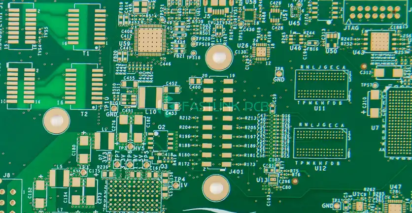
Silkscreen in PCBs refers to the printed layer on the board’s surface that provides vital visual information for manufacturing, assembly, testing, and maintenance. This layer typically features component reference designators, test point labels, polarity indicators, and assembly instructions—crucial aids for ensuring precise placement and efficient troubleshooting.
1.Enhancing Assembly Efficiency
The silkscreen layer clearly marks component locations and orientations, guiding pick-and-place machines or manual assembly to significantly reduce placement errors. For instance, silkscreen can indicate the exact pad for resistors or diodes and their polarities, ensuring correct placement on the first pass.
PCB Silkscreen Layer Overview | |
| Term | Description |
| Component Identifiers | Reference designators, part numbers, and values for placement and assembly |
| Component Outline | Physical outlines of component packages (e.g., BGA, QFP) |
| Board Information | Board title, revision number, and manufacturer details |
| Logos & Text | Company logos and branding information |
| Special Markings | Date codes, copyright notices, and approval stamps |
| Solder Mask Clearance | Gaps in the solder mask around pads to prevent solder bridges |
| Fiducial Marks | Alignment targets for automated placement and secondary operations |
| Board Zones | Defined regions such as analog, high-speed digital, power domains |
| Assembly Notes | Placement instructions and handling precautions |
| Test Points | Locations marked for probe or fixture contact during testing |
2.Facilitating Testing and Repair
By printing test point identifiers and probe locations on the silkscreen, technicians can quickly locate critical signal nodes, shortening diagnosis time. Clear reference designators also help repair engineers swiftly identify and replace faulty components.
3.Enhancing Aesthetics and Brand Recognition
Beyond functional annotations, the silkscreen layer can dramatically elevate a PCB’s visual appeal by incorporating custom graphics, brand logos, and color accents. Multi-color silkscreen printing is increasingly adopted in premium electronics. In consumer electronics, smart home devices, and wearables—where aesthetics are paramount—a thoughtfully designed silkscreen aligns the board’s look with product packaging and user interfaces, boosting brand cohesion and user perception.
Comparison of 4 Common PCB Silkscreen Processes
 PCB silkscreen layers can be produced using several imaging techniques—Liquid Photo Imaging (LPI), dry-film exposure, inkjet printing, and Laser Direct Imaging (LDI). Each method offers distinct trade-offs in resolution, layer thickness, durability, and cost, and should be selected based on specific application requirements.
| Process | Principle & Workflow | Resolution | Abrasion Resistance | Layer Thickness | Pros & Cons |
| Liquid Photo Imaging (LPI) | Photo-sensitive ink with photomask exposure followed by wet chemical development | high | Good | 0.35–0.85 mil | Industry standard with high resolution; higher cost & complexity |
| Dry-Film Exposure | Lamination of photosensitive resin film, exposure, then development | relatively low | Excellent | 0.5–5 mil | Wider line/space capabilities; flexible for multi-color use |
| Inkjet Printing | Direct deposition of silkscreen ink via inkjet nozzle, no mask needed | relatively low | Poor | 0.1–0.3 mil | Low cost, fast turnaround; limited durability & resolution |
| Laser Direct Imaging (LDI) | Direct laser ablation or exposure of photoresist without ink or masks | 200 µm (≈8 mil) | Fair | Marks substrate directly
| Simplified workflow; supports mixed inks; high equipment investment |
Key PCB Silkscreen Design Guidelines
In PCB layout, the silkscreen layer must balance readability, manufacturability, and error-proofing. The following four considerations are essential to ensure high-quality silkscreen and streamlined assembly.
1.Text Size & Placement
In PCB silkscreen design, text size and placement are the foremost considerations. To ensure readability during assembly, testing, and repair, silkscreen text should be at least 1 mm tall and maintain a minimum 5 mil (approx. 0.127 mm) clearance from component pads or vias.
2.Color & Contrast
Color and contrast dictate the legibility of silkscreen legends. A common scheme is white text on a green or black substrate, providing high contrast to help technicians quickly locate components and test points. Designers should also choose inks brand resistant to fading based on the PCB substrate and silkscreen process to ensure long-term visibility.
| FastlinkPCB Silkscreen Ink Models and Specifications | ||
| Model | Color Options | Description |
| KSM-S6188 | Green, White, Black, Blue, Red, Purple | Liquid photosensitive solder resist ink |
| KSM-P3188 | Natural | Liquid photosensitive circuit ink (fast-dry type) |
| KSM-P3228 | Natural | Liquid photosensitive circuit ink (slow-dry type) |
| KSM-P2006 | Natural | Liquid photosensitive circuit ink (screen-print type) |
| KSM-150 | White, Black, Yellow | UV-cured marking ink |
| HT-50 / HT-30 | Green, White, Black, Blue, Red | Liquid photosensitive solder resist ink |
| HT-10 | White, Black | UV-cured marking ink |
| Note: Our company can also source inks from TAIYO (Japan) PSR2000 series and TAMURA (Japan) DSR2200C series. | ||
3.Other design considerations
- High voltage and hazardous areas: Place safety warnings and high voltage markings outside of hazardous areas to prevent inadvertent operation.
- Future production compatibility: for spare devices that may be replaced, reserve multiple lines of reference markings in the same location.
- Multi-functional zones: multiple reference marks side by side to meet different versions or testing needs.
- Fine-pitch devices: use smaller text and line widths as needed to ensure readability.
- Heat dissipation management: additional solder resist dams around heat generating components to prevent interference with ink and solder flow.
- Multi-language translation: if for international markets, multi-language silkscreen can be designed in the same area for easy localization and maintenance.
Final Thoughts
PCB silkscreen design encompasses many critical details. To ensure your Gerber files integrate seamlessly with production workflows, we strongly recommend a joint review and optimization session with your manufacturing and assembly partners upon design completion.
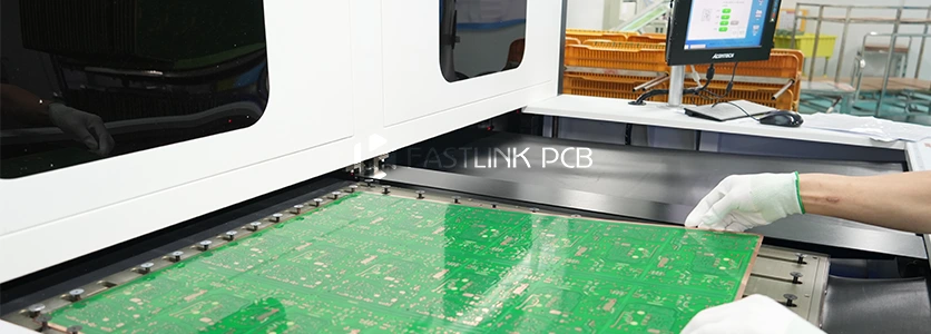
With 15 years of PCB fabrication expertise, FastlinkPCB not only masters high-precision silkscreen processes—such as LPI, LDI, and inkjet printing—but also offers comprehensive one-stop PCB services, from design review and rapid prototyping to volume manufacturing and final assembly, ensuring worry-free delivery of high-quality circuit boards.