- On October 31, 2025
- In blog
What You Need to Know About PCB Antennas: Advantages, Types, and Design Tips
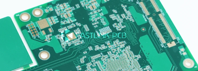
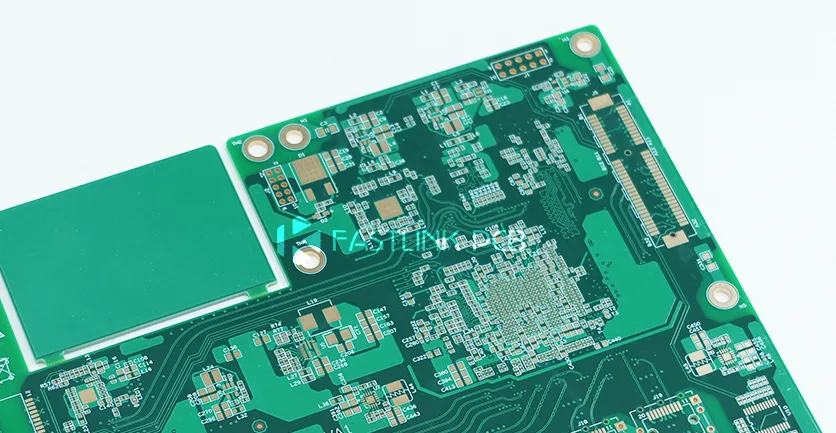
In modern wireless communication devices, antennas are indispensable core components. As devices continue to evolve toward greater miniaturization and integration, traditional external antennas are gradually being replaced by more compact solutions. PCB antennas (also known as board-mounted or embedded antennas) represent such an innovative design, directly integrated into the printed circuit boards of electronic devices.
Advantages of PCB Antennas
- Compact Size: PCB antenna designs enable extremely small dimensions, saving valuable space and meeting the needs of various compact devices.
- Superior Performance: When properly designed and reliably manufactured, PCB antennas deliver stable and excellent wireless connectivity.
- Low Power Consumption: PCB antennas are essentially engineered for low-power applications. This helps extend device battery life—particularly critical for wearables and other portable devices.
- Durability: Typically integrated within the device, PCB antennas are more robust than external antennas. Their non-exposed nature reduces damage risk, enhancing device durability and lifespan.
- Easy Integration: PCB antennas can be directly integrated onto the device circuit board, eliminating the need for additional external components or connectors and simplifying the manufacturing process.
- Versatility: PCB antennas offer broad applicability, suitable for nearly all electronic devices requiring wireless communication. They are found in everyday smartphones, laptops, IoT devices, and wireless sensors.
- Customizability: PCB antenna design offers high flexibility, allowing customization to specific application needs (e.g., adjusting frequency bands, gain, radiation patterns).
- Aesthetic Design: Unlike traditional antennas, PCB antennas are integrated within the circuit board, resulting in a concealed appearance that preserves the device’s sleek and streamlined look.
- High Cost-Effectiveness: Compared to other antenna types, PCB antennas offer lower manufacturing costs. They eliminate the need for external antennas or complex embedded installation processes, effectively reducing production expenses.
Common Types of PCB Antennas

1.Monopole Antennas
Monopole antennas are relatively common, consisting of a single conductive element typically placed on the PCB surface and operating with an appropriate ground plane. These antennas generally employ an omnidirectional radiation pattern, meaning signals propagate uniformly in all directions. Advantages of monopole antennas include simple structure, ease of integration, and low cost.
2.Patch Antennas
Patch antennas employ a planar structure, with a conductive patch placed on one side of the PCB and a ground plane on the opposite side. Unlike monopole antennas, this design focuses signal radiation direction, providing higher gain.
3.Dipole Antenna
As the name suggests, a dipole antenna consists of two conductive elements, typically arranged vertically on a printed circuit board. Compared to other antenna types, it offers superior radiation balance characteristics, enabling polarization diversity or beam control.
4.Loop Antenna
A loop antenna operates through a closed conductive element, featuring a compact and efficient design. It is widely used in radio frequency identification (RFID) and specific radio applications.
Differences Between PCB Antennas and Wired Antennas
Wired antennas are typically large in size, mounted externally on devices, and usually made of conductive materials like copper or aluminum. They are designed to resonate at specific frequencies. Such antennas are suitable for devices requiring strong signal transmission and are commonly found in radio systems, base stations, and other long-range communication equipment. Due to their size, wired antennas often require more space, increasing installation and production complexity.
In contrast, PCB antennas feature an extremely compact design, directly integrated onto the device’s circuit board, making them suitable for small-sized equipment. While their power output may be weaker than that of wired antennas, it is sufficient to meet medium-to-short-range communication needs. Their core advantages lie in saving space, reducing costs, and simplifying device design.
Differences Between PCB Antennas and Chip Antennas
Although chip antennas (also known as surface-mount antennas) and PCB antennas are both integrated antenna solutions, they differ in design and application. Chip antennas are typically smaller in size, mounted on the surface of a PCB, and made from materials such as ceramic or ferrite. The surface-mount antenna integration process is relatively simple, offering good radiation efficiency and impedance matching characteristics. They are suitable for space-constrained applications requiring thin profiles, such as smartphones and wearable devices.
PCB antennas, however, are directly integrated onto the circuit board via printing or etching processes, formed concurrently during PCB manufacturing. These antennas are suitable for devices requiring higher antenna gain and coverage, such as routers and access points. Compared to surface-mount antennas, PCB antenna design and integration are more complex, necessitating comprehensive consideration of multiple factors including PCB material, dimensions, shape, and ground plane.
PCB Antenna Design Techniques: Key Methods for Enhancing Performance
When designing PCB antennas, beyond fundamental design considerations, numerous details can effectively boost antenna efficiency and ensure superior wireless performance. Below are common optimization techniques that help designers enhance the output efficiency of PCB antennas.
1.Utilize Matching Networks for Tuning
Matching networks are key to antenna tuning. They compensate for factors that may degrade antenna performance, ensuring impedance matching between the antenna and the circuit.
2.Select an Appropriate Ground Plane
An improper ground plane can cause signal crosstalk and reduce signal quality.
3.Optimize Antenna Placement
PCB edges typically offer the best location for antenna placement. Avoid positioning antennas near metal or plastic surfaces, as these materials suppress antenna signals. Plastic materials, in particular, exacerbate signal loss due to their higher dielectric constant, negatively impacting transmission quality.
4.Selecting Premium PCB Materials
Opting for high-quality FR-4 material is a prudent choice. Inferior FR-4 can cause significant power loss in PCB antennas due to thermal issues, severely compromising performance. To optimize antenna performance, designers should consider multiple factors including material quality, low loss tangent, and appropriate dielectric constant.
5.Meticulously Design PCB Layout
Effective PCB layout design significantly enhances antenna performance. Poor layout exacerbates interference and reduces antenna efficiency. Designers often overlook matching networks, which can cause severe power reflection.
6.Professional Testing and Optimization
To ensure design effectiveness, collaboration with RF and antenna technology experts during the testing and validation phase is recommended. For specialized support, FastlinkPCB is your trusted technical partner. With extensive experience in RF design and PCB antenna optimization, contact us today!