- On January 4, 2024
- In blog
The Role of Laser Drilling in HDI-PCB Manufacturing
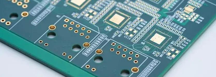
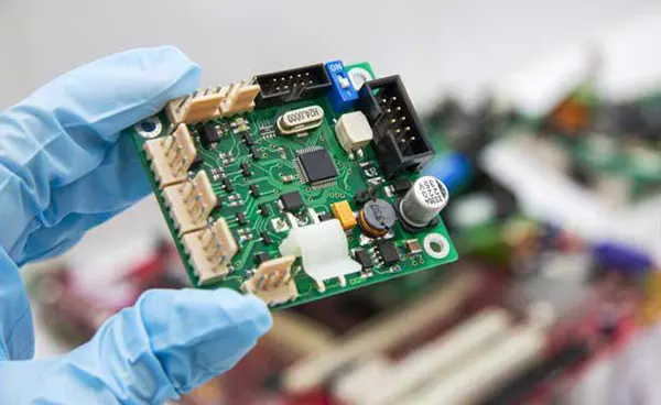
High-density interconnect (HDI) printed circuit boards (PCBs) are a type of PCB that features very small traces and vias, which allows for more compact and powerful electronic designs. HDI PCBs are used in a wide range of applications, including smartphones, laptops, and medical devices.
Laser drilling is a key process in the manufacturing of HDI PCBs. It is used to create the small traces and vias that are essential for HDI design. In this article, Let’s delve into understanding the role of laser drilling in HDI-PCB manufacturing, along with other crucial details.
About Laser Drilling
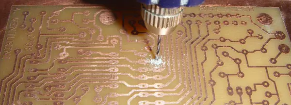
Laser drilling involves using high-intensity laser beams to create precise holes in PCB substrates. Laser drilling offers greater flexibility and precision, unlike traditional mechanical drilling methods, making it ideal for intricate HDI-PCB designs. The laser beam is directed onto the target area, where it vaporizes the material, leaving behind a clean and accurately sized hole. This non-contact drilling process ensures minimal stress on the delicate PCB substrates, reducing the risk of damage.
The Laser Drilling Process
Laser drilling is a non-contact process that uses a laser beam to melt or vaporize the material being drilled. The laser beam is focused onto the surface of the material, and the heat from the beam causes the material to melt or vaporize. The melted or vaporized material is then removed, leaving a hole in the material.
The laser drilling process for HDI PCBs is typically carried out in two steps:
● Pre-drilling: The first step is to create a pilot hole in the material. This pilot hole is used to guide the laser beam during the second step.
● Drilling: The second step is to use the laser beam to create the final hole. The laser beam is focused on the pilot hole, and the heat from the beam causes the material to melt or vaporize. The melted or vaporized material is then removed, leaving the final hole in the material.
The following is a video of a pulsed fiber laser drilling holes in a PCB circuit board:
Benefits of Laser Drilling in HDI-PCB Manufacturing
The adoption of laser drilling in HDI-PCB manufacturing offers multiple benefits. For example, it can make electronic devices more miniaturized. The precision of laser drilling ensures that the holes are clean and well-defined, thus preserving the structural integrity of the circuit board and lowering the risk of failure.
Micro-Vias and Miniature Holes
Laser drilling excels in creating micro-vias, which are tiny holes with diameters ranging from a few micrometers to tens of micrometers. These micro-vias enable the interconnection of multiple layers within the HDI-PCB, facilitating the high-density integration of components. Laser drilling also allows the fabrication of miniature holes with exceptional precision, enabling the use of smaller components and enhancing the overall circuit density.
Improved Accuracy and Alignment
The laser drilling process offers superior accuracy, allowing for precise positioning and alignment of holes. This is crucial in HDI-PCB manufacturing, where the spacing between components and the alignment of vias play a vital role in ensuring optimal signal integrity and electrical performance. Laser drilling ensures consistent and repeatable hole placement, reducing the risk of misalignment and improving the overall reliability of the PCB.
Increased Design Flexibility
HDI-PCBs demand intricate designs with complex interconnections and tight spacing. Laser drilling provides designers with greater flexibility in creating intricate patterns and interconnects. The ability to place holes precisely at different angles and positions allows for more efficient routing and optimized use of space, ultimately enabling the development of smaller and more compact electronic devices.
The Role of Laser Drilling in HDI PCB Manufacturing
The essence of HDI technology lies in its ability to place more components on both sides of the raw PCB substrate. A critical aspect of this process is creating microvias – tiny holes that form electrical connections between the layers in a multilayer PCB. These microvias are significantly smaller than traditional vias and require precise and controlled methods for creation, which is where laser drilling comes into play.
Laser drilling offers several advantages over traditional mechanical drilling, including:
● Accuracy: Laser drilling can create very precise holes with tight tolerances. This is essential for HDI design, which requires very small traces and vias.
● Speed: Laser drilling is faster than mechanical drilling, which can reduce production costs. This is important for HDI PCBs, which are often used in high-volume production.
● Reliability: Laser drilling is a more reliable process than mechanical drilling, which can reduce the risk of defects. This is important for HDI PCBs, which are often used in critical applications.
Laser Drilling Applications in HDI-PCB Manufacturing
Multi-Layer HDI-PCBs
By creating micro-vias and through-holes, laser drilling facilitates the interconnection of various layers, enabling the efficient flow of signals and power across the PCB. This is particularly beneficial in applications where space is limited, such as smartphones, tablets, and wearables.
High-Speed Communication Systems
In high-speed communication systems, such as data centers and telecommunications equipment, signal integrity is of utmost importance. Laser-drilled micro-vias enable high-density interconnects, minimizing signal loss and ensuring reliable transmission of data at high frequencies. The precise hole placement and alignment achieved through laser drilling contribute to the overall performance and integrity of the communication systems.
Considerations in Laser Drilling for HDI-PCBs
Material Selection
The choice of PCB substrate material is crucial in laser drilling. Different materials have varying absorption properties for laser energy, which can affect the efficiency and quality of the drilling process. Proper selection of materials, such as specialized laminates and high-temperature substrates, ensures optimal laser drilling results.
Thermal Management
Laser drilling generates heat during the process, which can impact the integrity of the PCB substrate and surrounding components. Adequate thermal management techniques, such as controlled laser parameters and cooling mechanisms, must be implemented to prevent excessive heat accumulation and minimize any potential damage.
Conclusion
Laser drilling is a key process in the manufacturing of HDI PCBs. By understanding the role of laser drilling and considering the key factors involved, manufacturers can harness its benefits to produce cutting-edge HDI-PCBs that drive innovation in the electronics industry.
Leave a comment